Buried lateral current confinement for improved efficiency of diode lasers
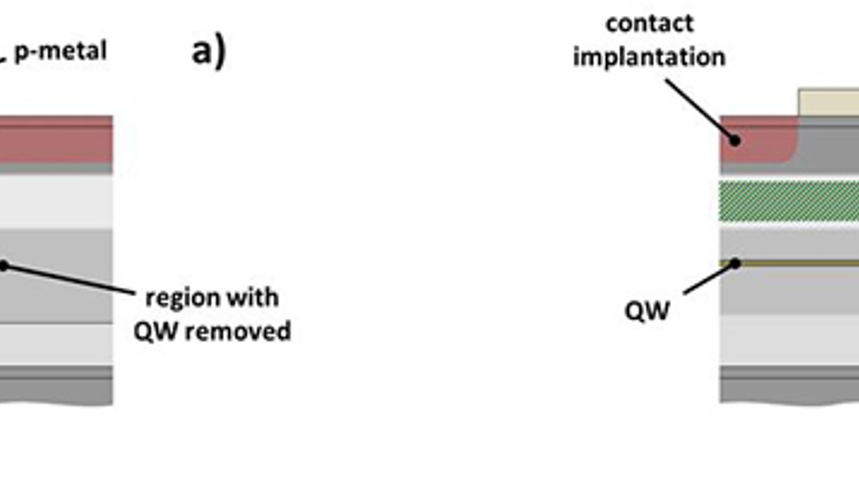
Fig. 01. cross section schematic of a buried-mesa laser (a) and a lateral buried implantation laser (b).
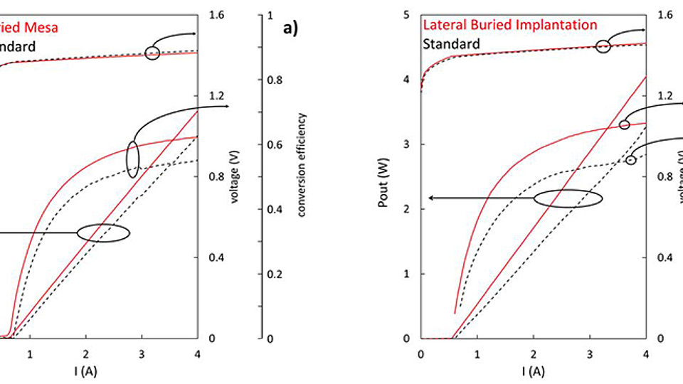
Fig. 02. PVI curves of a buried mesa laser (a) and of a lateral buried implantation laser (b). In each case, a comparison is made with a standard laser fabricated with the same vertical structure (dashed lines).
Improving efficiency and brightness of laser diodes are key targets for high- power laser systems in order to reduce the cost per usable photon. This holds for direct diode systems as well as for diode pumping of fiber or solid- state lasers.
Current spreading and loss of carriers to regions which do not reach the threshold carrier density are effects that limit device efficiency. Accumulation of carriers at the edges of the active region, which again is related to current spreading, results in reduced beam quality in lateral direction, which limits the coupling efficiency e.g. into fibers. Introducing buried current apertures can thus increase both efficiency and beam quality.
Two alternative technological approaches are currently pursued at FBH to realize these features, both based on 2-step epitaxial growth. In either case, the vertical structure is grown up to a position in the p-waveguide part above the active region.
In the buried mesa approach the active region is then removed by etching except for the intended gain regions. Thus, absorption as well as gain is eliminated from the sides of the laser stripe. If the active region is also removed from the regions close to the facets, this can enhance the resistance against catastrophic optical mirror damage (COMD), allowing for higher maximum operation power and improved reliability. The vertical structure is then completed in a second growth step. The procedure starts on a patterned, non-planar surface which comes along with challenges like local composition modulation in ternary layers or the exposure of different materials at the sidewalls of the remaining active region. This is especially problematic if Al-containing layers are involved.
The second approach keeps the surface planar and the current aperture is created by implanting Si or O around the active laser stripe. The second growth step removes the crystal damage and activates the dopants so that highly resistive regions are formed.
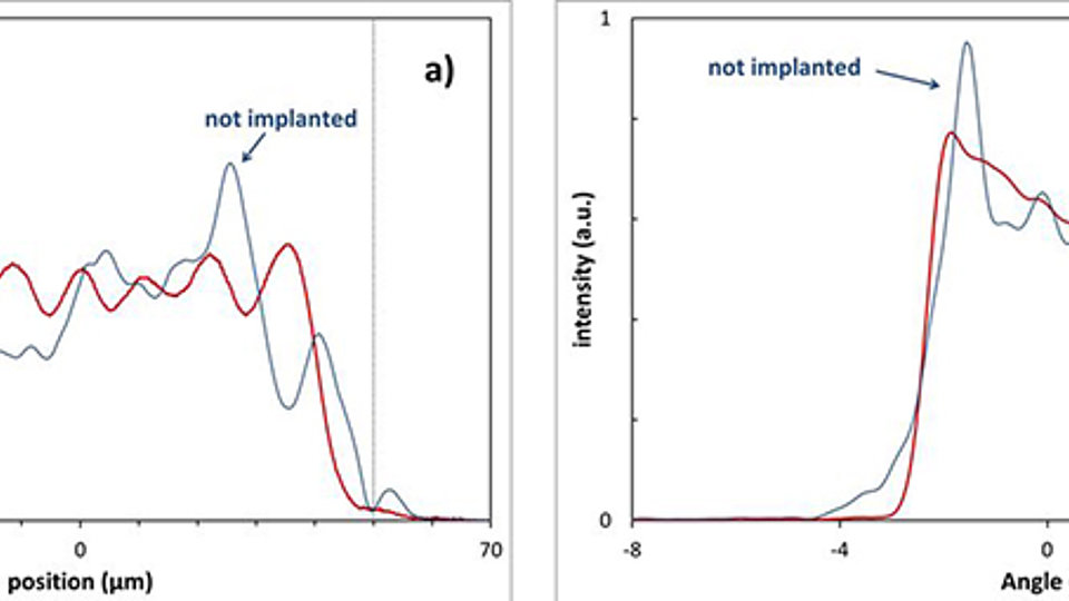
Both approaches result in reduced threshold current and higher slope efficiency compared to reference standard devices. Together, this yields a gain in overall efficiency. For the buried mesa approach also a higher COD threshold has been confirmed when the active region is removed at the facets. With implanted current aperture beam quality is improved thanks to a more top-hat shape of the near-field lateral profile, the absence of side lobes and a reduced far-field width. This translates into more efficient coupling of the emitted light into optical fibers.
Publications
P. Della Casa, O. Brox, J. Decker, M. Winterfeldt, P. Crump, H. Wenzel and M. Weyers, "High power, broad area, buried mesa lasers", Semicond. Sci. Technol. 32 065009 (2017)
D. Martin, P. Della Casa, T. Adam, C. Goerke, A. Thies, K. Häusler, O. Brox, H. Wenzel, P. Crump, M. Weyers and A. Knigge, "Current Spreading Suppression by O- and Si-Implantation in high Power Broad Area Diode Lasers", Photonics West LASE 2019 paper 10900-19


