Vertical GaN Transistors
Power semiconductor devices are utilized in power conversion systems and as drivers for high power optical laser systems. For such devices, a vertical topology is favorable since it combines thick epitaxial layers for blocking high voltage in off-state and very high current density for low resistance during on-state. Moreover, this topology offers low energy consumption and, using the bulk semiconductor, an enhanced thermal dissipation. We made significant progress in exploring and developing vertical transistors based on gallium nitride (GaN) – demonstrating transistor structures with extremely compact dimensions that push the boundaries to what is currently possible.
Advantages of a vertical device design
Until recently, GaN-based power electronic devices used a lateral configuration due to the superior conduction properties of its lateral two-dimensional electron gas. In the future, however, there will also be a large market for vertical GaN devices. For higher operation voltages, such as 1200 V and above, vertical device concepts have distinct advantages as the voltage drops all across the substrate at off-state. This eases design and implementation of high-voltage power switches. They can be, for example, implemented in future electromobility as well as electric aircraft propulsion systems and many other applications. Furthermore, they can be used for direct high-speed laser driving using chip-on-chip integration. In any case, reliability is key. Therefore, FBH developments focused on extremely low defective free standing highly conductive GaN substrates. In a first approach, we concentrated on the vertical gate drive mechanism and verified this technology for pulsing diode lasers.
Fast vertical laser drivers for LiDAR applications
Very high acquisition-rate long-range LIDAR systems, used for example for autonomous driving, require fast laser driving along with high-power supply electronics. The integration of GaN-based power electronics enables very fast laser drivers with high current densities. Conventional laser assembly architectures do not fulfill these requirements, and thus a new architecture is essential.
We have developed a concept for a chip-on-chip integration of a diode laser with a vertical GaN transistor serving as a fast driver.
Concept for the chip-on-chip integration
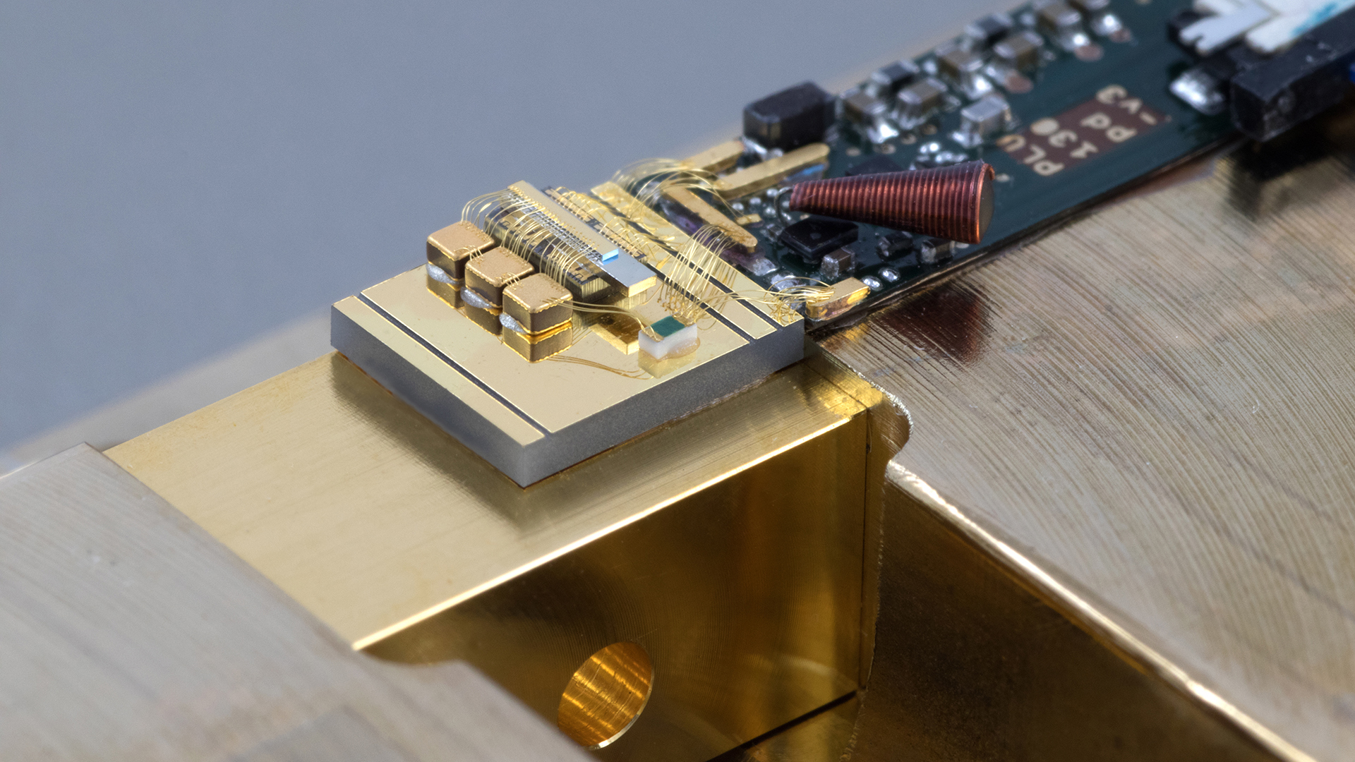
We introduced the concept of chip-on-chip integration of the laser diode mounted on a driving GaN-based power transistor, side by side with very fast high-current energy storage, generating short and powerful laser pulses. New vertical GaN switching transistors have been developed and manufactured on highly conductive free standing GaN substrates for this innovative assembly concept.
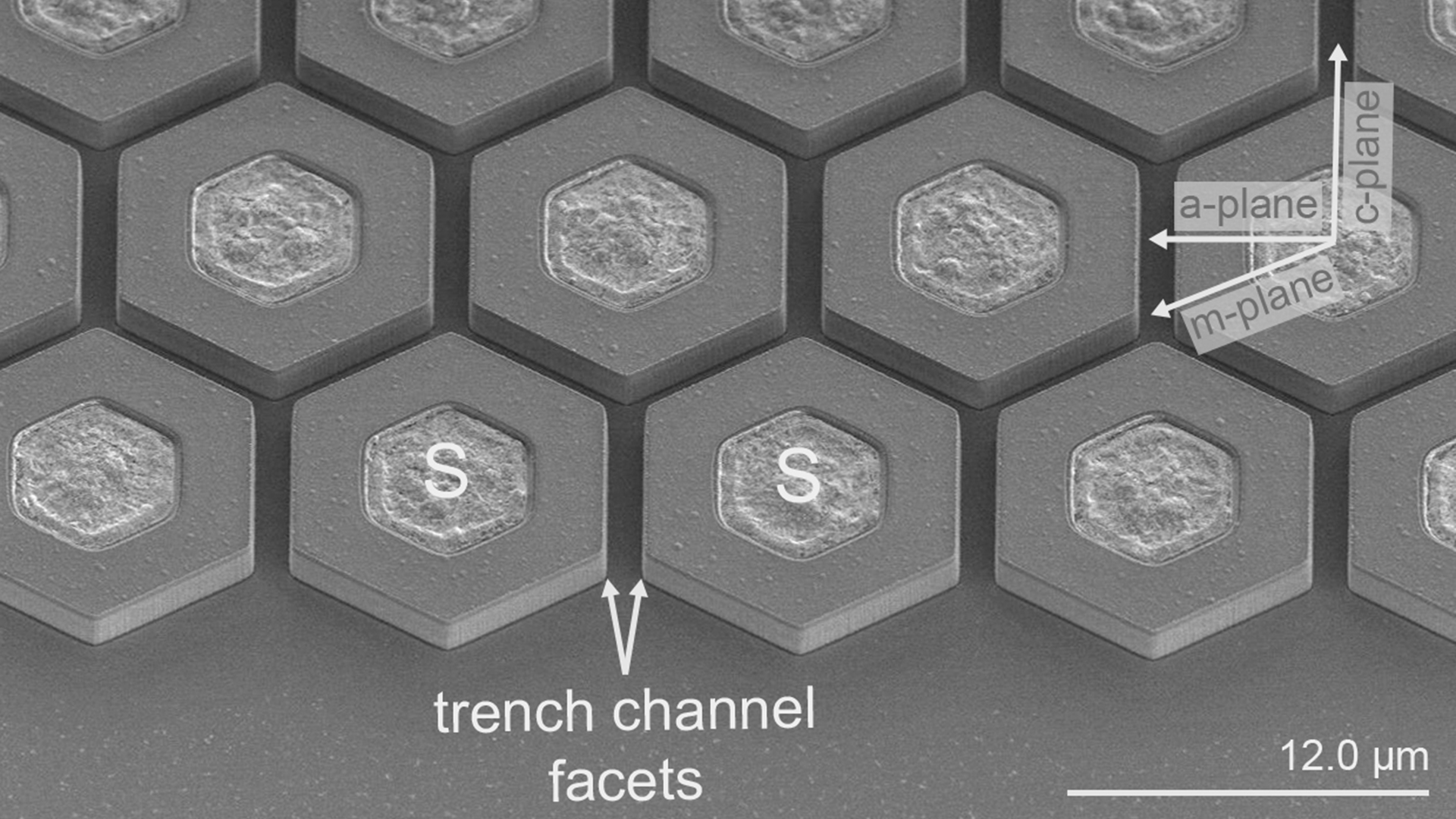
To lay the foundation, we first studied the influence of substrate type and vendor as well as the gate drive technology on the transistor switching properties. The transistors have been processed on different substrates with a gate channel orientation along the two GaN non-polar crystal planes, a- and m-plane. The substrates differ in terms of technology and defect density. Low defective ammonothermal substrates were compared to medium defective hydride vapor phase epitaxy (HVPE) substrates.
It was found that the best performing devices, with a maximum output current above 4 kA/cm2 and an area specific on‑state resistance of 1.1 mOhm∙cm2, are manufactured on ammonothermal GaN substrate with the gate channel parallel to the a‑plane of the GaN crystal. These large periphery switching transistors, with 142 mm gate width and 305 mOhm on-state resistance, were directly combined with a diode laser chip by applying a chip-on-chip mounting technology. The whole arrangement has then been placed on a low-inductance thermally conductive but insulating AlN ceramic board. The demonstrator enabled 3.6 ns laser pulses at 904 nm emission wavelength and a peak optical power of 4 W.
