Gallium Nitride-Based Microwave Processes
We offer GaN-based MMIC processes for customized circuit designs in several frequency bands.
X- and Ka-band GaN MMICs
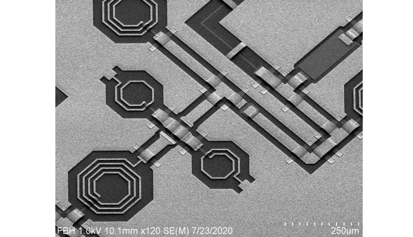
The available processes in 0.25 µm and 0.15 µm gate technology on SiC substrate are based on proven process modules and suitable for GaN MMICs in the 5 to 40 GHz range. Structures for small signal applications as well as transistor cells for high power amplifiers in the mentioned frequency range are available as active components. As passive components, thin film resistors, MIM capacitors, spiral inductors, substrate vias and microwave lines (coplanar and microstrip) can be integrated. A model library for active and passive elements is available for flexible GaN MMIC design. Static, dynamic and RF measurements can be performed after processing on-wafer or with packaged devices.
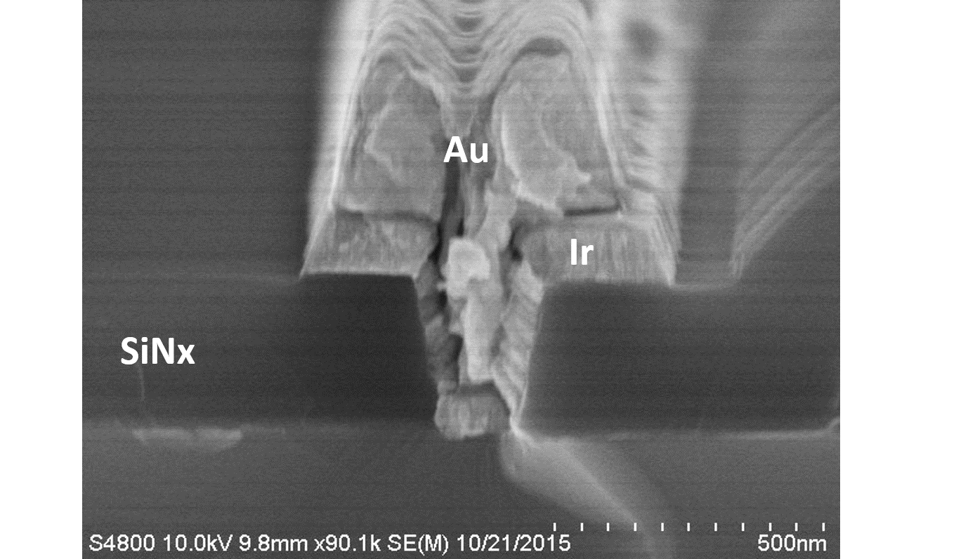
As a worldwide unique selling point, our GaN MMIC process contains a special gate technology based on a metal sputtering process (iridium). It significantly reduces dispersion effects and increases the long-term reliability of the active devices.