(Al,In)GaN-based LEDs & diode lasers
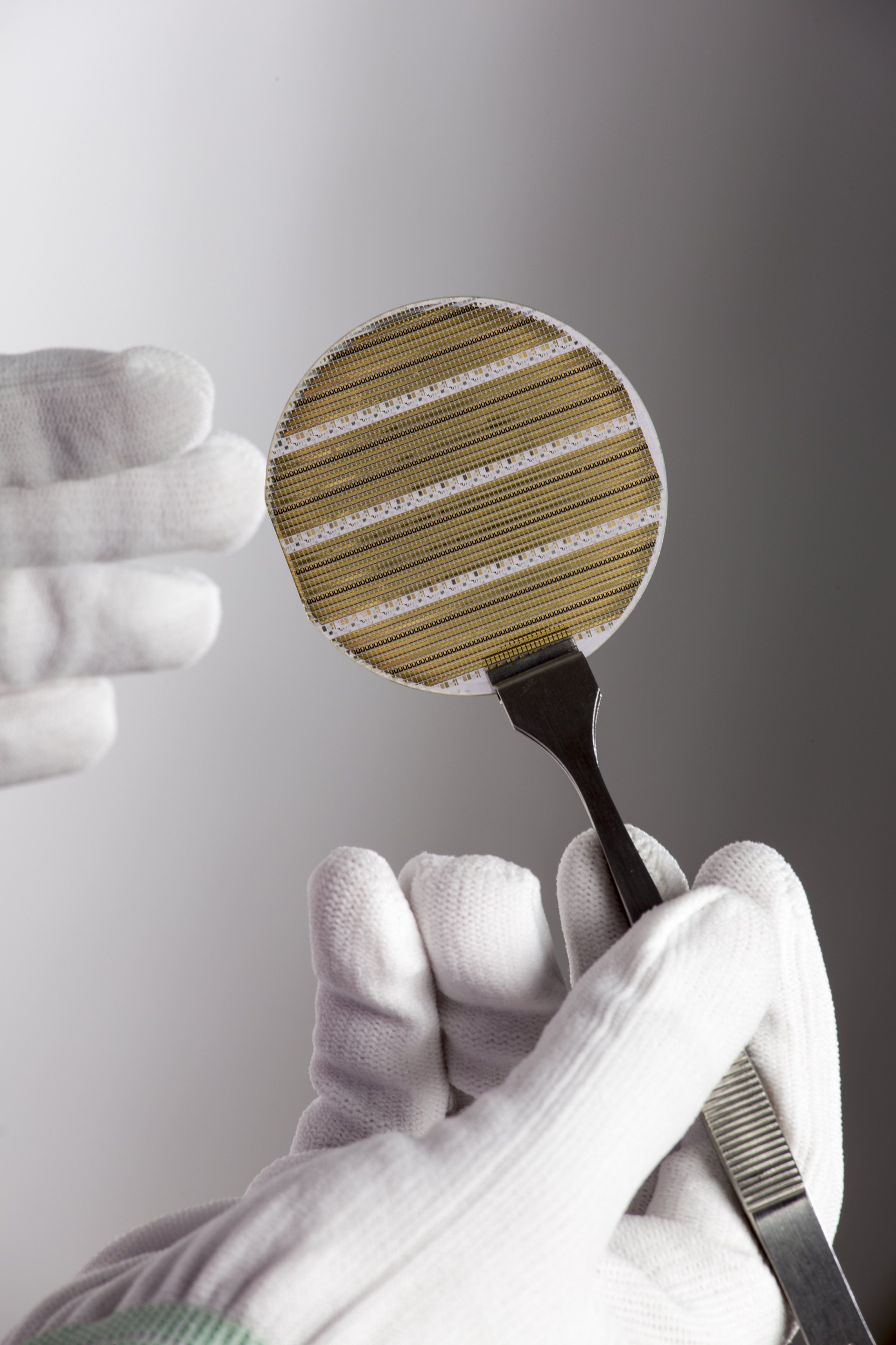
In our cleanrooms we operate process lines to develop and fabricate (Al,In)GaN-based LEDs and diode lasers with different emission wavelengths. UVB and UVC LEDs use sapphire substrates, while (In)GaN-based RW, DFB and DBR diode lasers use GaN substrates.
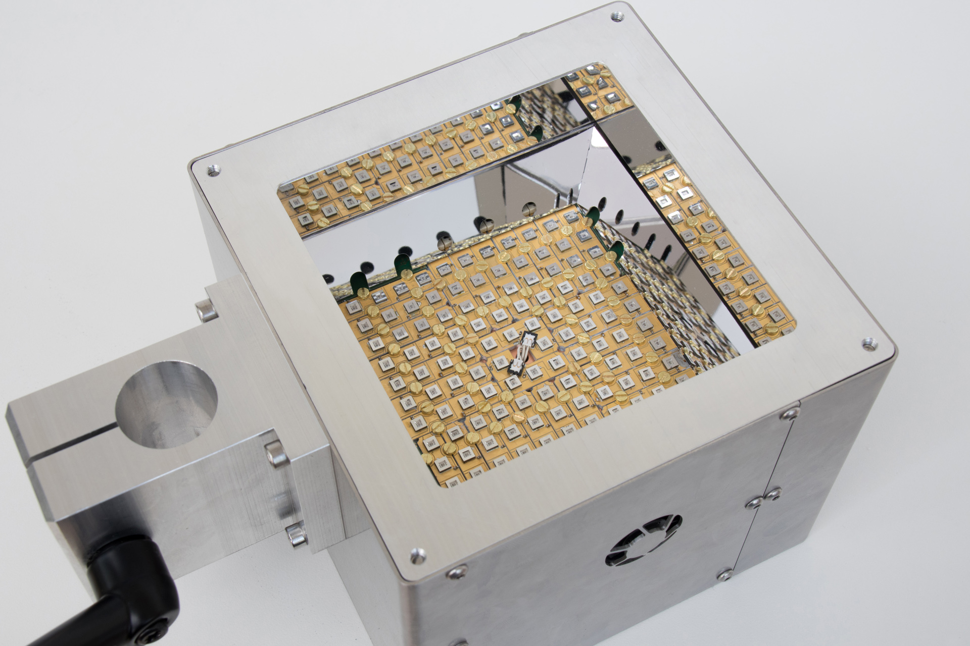
In addition to the individual process steps, we also offer epitaxy of layer structures, including their characterization. Moreover, we design and manufacture modules and systems as prototypes or demonstrators so that customers can test our UV LEDs in their applications.
Processes and methods
We are working on (Al,In)GaN-based UV LEDs and diode lasers in our cleanrooms, which are operated by the Materials Technology, Process Technology and Mounting & Assembly Technology departments. For this purpose, we use processes that are specially adapted to these devices:
- Fabrication of single crystalline AlN base layers on 2" sapphire substrates using MOVPE, sputtering, high temperature annealing, micro structuring and lateral overgrowth
- Epitaxy of (InAlGaN)N:(Si,Mg) layer structures on 2" AlN/sapphire templates and 2" GaN substrates using MOVPE
- Contact, projection and electron beam lithography
- Deposition of metals for p- and n-contacts
- Sputtering and PECVD for the deposition of insulator layers
- Plasma etching for the realization of mesa structures and waveguides
- Backend processes (thinning, scribing and breaking) to separate wafers into chips
- Coatings of laser facets by ion beam sputtering
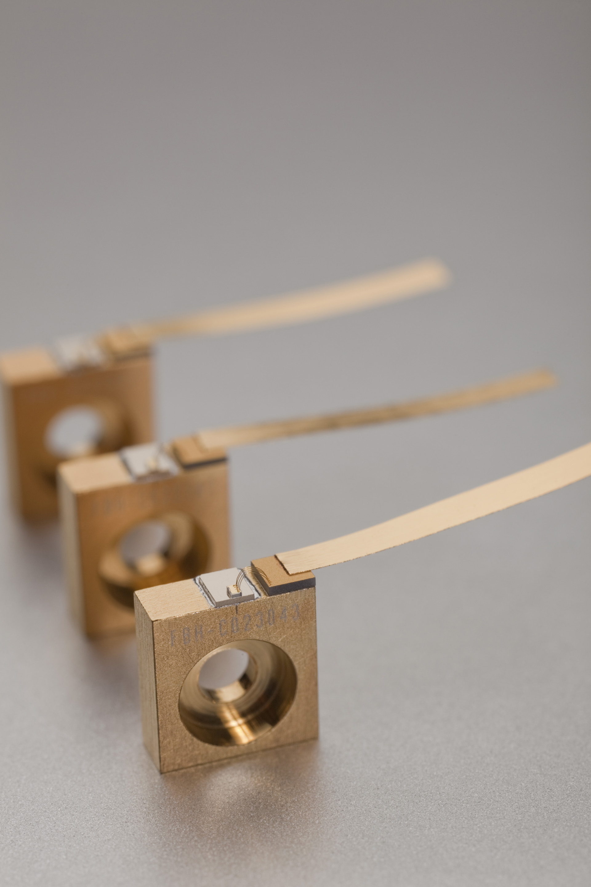
- Mounting of chips on submounts, heat sinks or in suitable packages