InP-on-BiCMOS Heterointegration
For system integration, terahertz circuits must be realized and connected , for example, to antenna structures. These structures and interconnections must maintain the highest possible bandwidth, should exhibit low losses, reproducibly match the model, and be inexpensive to manufacture.
We offer two different approaches to realize THz systems:
InP-DHBT-SiGe-BiCMOS heterointegration on wafer level
We have further developed the transfer substrate concept for 3D integration of InP-DHBTs on SiGe-BiCMOS. In this process, the wafers are bonded together with their front sides, the InP substrate is then removed and vertical RF contacts are created to connect the subcircuits. This type of heterointegration combines the advantages of the two semiconductor technologies: complex analog and digital circuits in SiGe-BiCMOS can deliver high output power at high frequencies when combined with an InP-DHBT power amplifier. Different signal sources have been fabricated as technology demonstrators, providing output frequencies of currently up to 330 GHz.
We offer this process for external partners and customers together with the Leibniz Institute IHP (Frankfurt/Oder).
InP chip-based integration
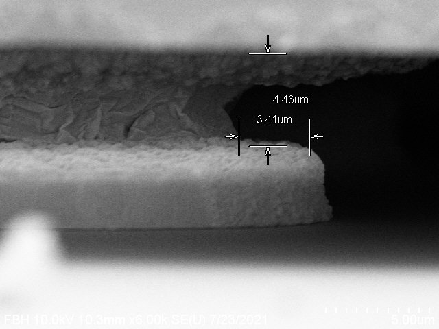
Classical bond wire interconnects beyond 100 GHz are difficult to control due to variations in manufacturing. We use flip-chip integration specifically for InP processes applying the in-house developed in-bump process. This enables multi-technology system designs with low thermal budgets (<200 °C), including passive multilayer carrier substrates with shielded waveguides, fabricated in a structure similar to the InP-HBT process. Passive and active InP-HBT circuits were mounted on the carrier substrates and measured to demonstrate the concept. They achieved a bandwidth from DC to 450 GHz, with an insertion loss of less than 1 dB per transition.