MicroLAB
No matter if it is a computer, mobile phone, ABS or airbag system, nearly every modern technical solution requires the tiny all-rounders developed from micro electronics and microsystems technology. The school lab MicroLAB explains and shows, how such micro devices are manufactured.

An aluminum layer is deposited onto the glass carrier before transferring the structure (©GenaU/Rasche)

Photoresist is applied on the glass carrier in order to structure the aluminum layer (©GenaU/Rasche)

The structure is transferred onto the glass carrier by exposure to UV light (©GenaU/Rasche)
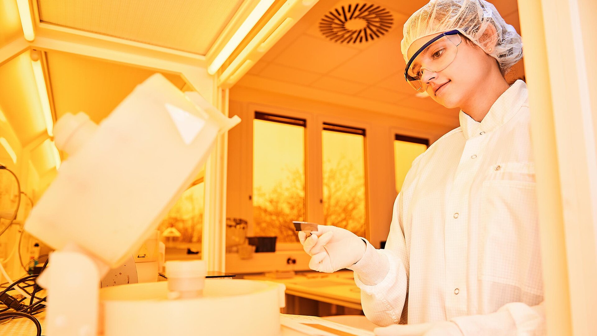
Trainee placing a wafer piece into a coating spinner (© Matthias Baumbach)

After exposure, the areas covered by resist remain, the surrounding areas are etched away in an acid bath (© Matthias Baumbach)

Trainee separating a large wafer into individual chips (© Matthias Baumbach)
The laboratory is run by Lise-Meitner-Schule and Ferdinand-Braun-Institut and combines practical experiments with an insight view into the work routine of a research institute. The presentation is held in German language.
MicroLAB is a member of GenaU, a network of Berlin and Brandenburg school laboratories.