GaAs Laser Diodes
In our clean rooms, we offer process lines for the production of ridge waveguide (RW), broad-area (BA) and tapered diode lasers as well as laser bars. In addition, we offer the associated process modules as well as BA short-loop processes to characterize the vertical laser layer structures grown by our epitaxy. For frequency-stabilized diode lasers (DFB and DBR lasers), we additionally introduce grating structures into the laser resonator.
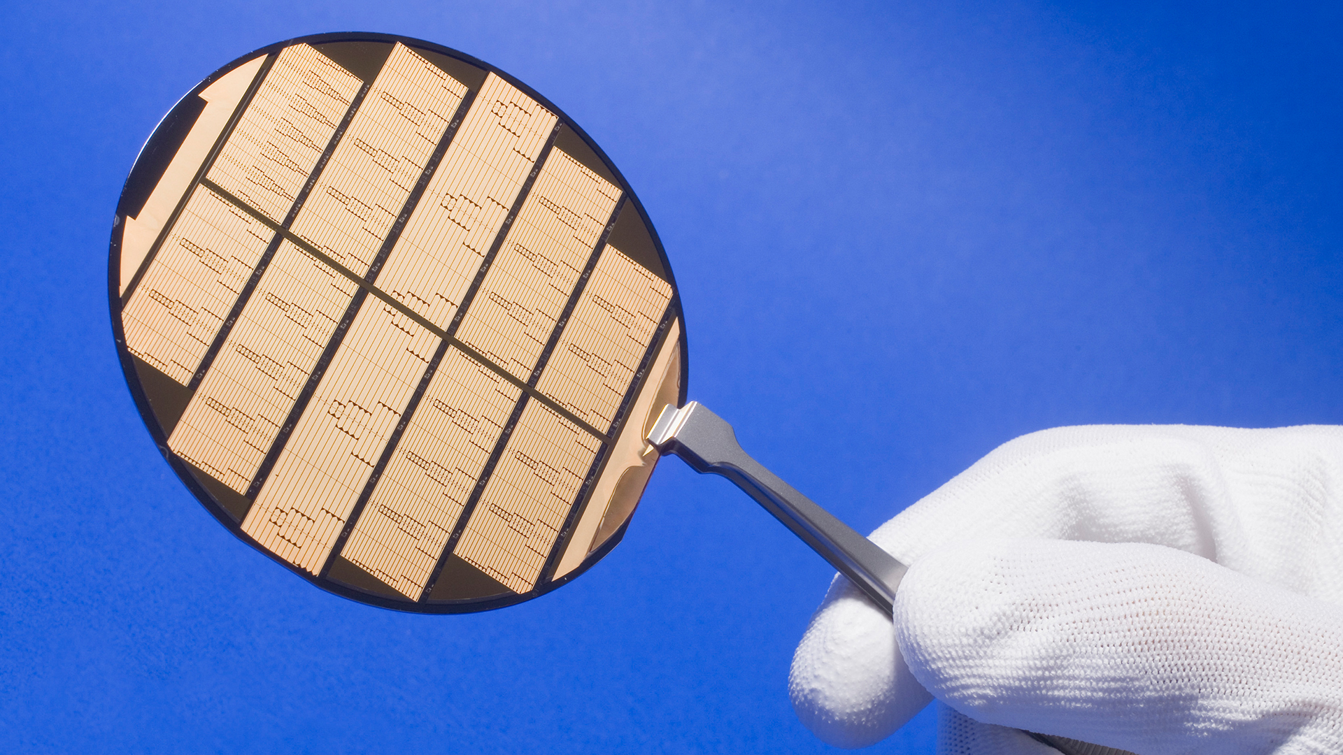
Processed 3 inch wafer
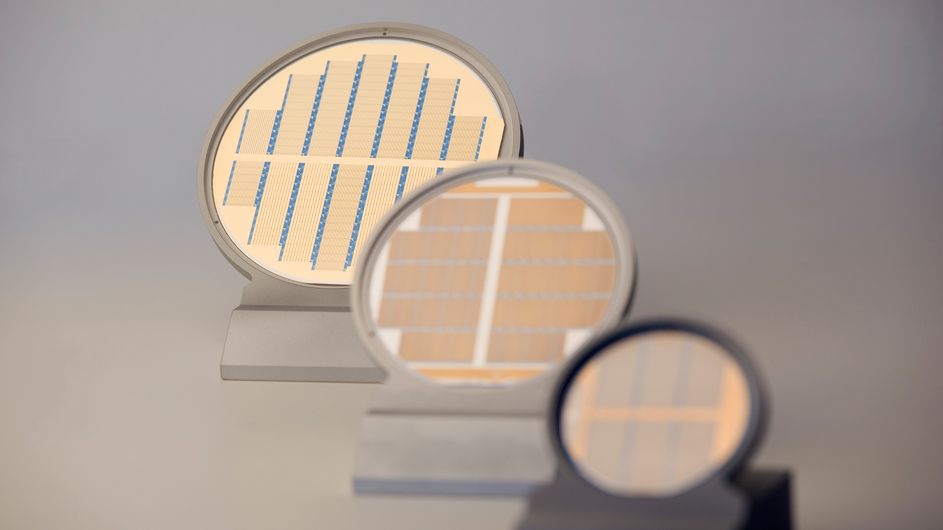
Processed 2-, 3- and 4-inch laser wafers
Processes and methods
We manufacture GaAs laser diodes in the clean rooms operated by the Process Technology department. For this purpose, we use individual process steps that are optimized for GaAs laser diodes.


- Contact and projection lithography including periodic structures with structure sizes down to 500 nm
- electron beam lithography for gratings and ridges with critical dimension (CD) of 70 nm
- ion implantation for current confinement
- wet and dry chemical etching processes for the realization of waveguides
- sputtering and PECVD for the deposition of insulator layers.
- evaporation and sputtering processes for p- and n-contacts
- electrochemical deposition of gold
- backend process (thinning, automated scribing and breaking)
- Separation of wafers into bars in ultra-high vacuum and passivation of the facet surfaces, by epitaxial coating (MBE) with zinc selenide, without leaving the ultra-high vacuum.
- Separation of wafers into bars under air with subsequent hydrogen plasma cleaning and passivation of the facet surfaces, by epitaxial coating (MBE) with zinc selenide, in ultrahigh vacuum.
- facet coatings by ion beam sputtering for reflectivities in the range ≤ 10-4 to > 98%.