Defect Engineering
Stacking different two-dimensional (2D) materials like graphene into vertical heterostructures is expected to lead to atomically thin electronic and sensing devices. These include ultra-steep slope tunneling transistors for low-power digital applications. Within the family of 2D materials, hexagonal boron nitride (h-BN) plays a central role in two ways: electronically, its large band-gap enables efficient electronic confinement as required in ultra-thin layers. On the other hand, its chemical inertness (i.e. the lack of dangling bonds) and high mechanical strength make it an ideal substrate or encapsulation layer for other 2D materials. Presently used preparation techniques such as mechanical exfoliation and stacking of 2D materials are hardly scalable and lack reproducibility. Therefore, the growth of 2D layers and heterostructures via van der Waals epitaxy (vdWE) is an attractive alternative.
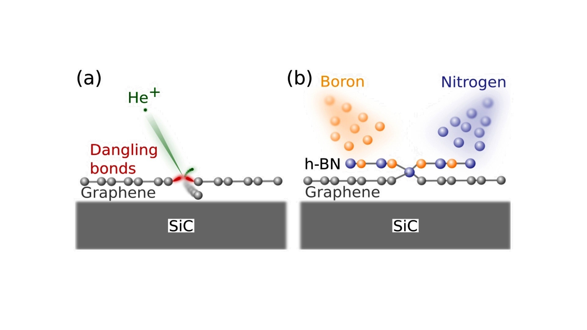
The central idea of this project is to utilize a focused ion beam (FIB) within a He ion microscope as a novel tool to deliberately create atomic-scale defects which in turn define the nucleation and layer orientation of h-BN. By ion beam irradiation, chemically active defects in graphene will be deterministically placed and engineered (as shown schematically in Fig. 1a). According to molecular dynamics simulation, irradiation of 2D materials with ions of noble gases with energies in the keV range results in the formation of defects with control down to single vacancies. These defects will act as nucleation centers for the tailored nucleation of h-BN via molecular beam epitaxy (MBE), see Fig. 1b. The experiments will be accompanied by theoretical modeling of the defect formation in graphene under ion irradiation and of the role of the underlying substrate. Furthermore, we will develop treatments of these irradiation-induced defects (IIDs) to control the nucleation of h-BN. The proceeding lateral formation of defect-free h-BN from IIDs will be tuned to form graphene/h-BN heterostructures with tailored properties.
To demonstrate the usefulness of our method, 2D heterostacks will be integrated into Hall bar structures to be characterized with respect for their use in quantum metrology. The design of the devices will be developed such that their active region is only formed of defect-free areas of the h-BN/graphene heterostructure. The fundamental knowledge and practical experience gained in this project will provide useful design criteria to further advance the scalable integration of 2D heterostructures into electronic devices via defect-controlled vdWE.
This project receives funding from the Leibniz Association within the framework of the Leibniz Collaborative Excellence Programme under grant no. K335/2020. The work is carried out in close collaboration with Paul-Drude-Institut für Festkörperelektronik, Helmholtz-Zentrum Dresden-Rossendorf, and with the CoreLab Correlative Microscopy and Spectroscopy of Helmholtz-Zentrum Berlin.