Indium Phosphide HBT Process
The terahertz region (0.1 - 3 THz) is located in the electromagnetic spectrum below the optical frequencies. To date, the terahertz band is mostly unused for a lack of suitable electronic components, which are commercially available only up to around 100 GHz. It is the aim of this project to establish a monolithic microwave integrated circuit (MMIC) technology to fill the THz gap. The aim of our work within the Joint Lab InP Devices is to provide a terahertz electronic technology for high-frequency integrated circuits (MMIC). We specifically translate fundamental materials research – with a focus on indium phosphide (InP) – into applied circuits and modules.


By means of 0.5 µm electron beam lithography, cutoff frequencies of fmax above 450 GHz at a breakdown voltage BVceo > 4.5 V could already be achieved. Integrated high-frequency circuits (amplifiers, mixers, oscillators) have been demonstrated in the frequency range from 100 to over 300 GHz.
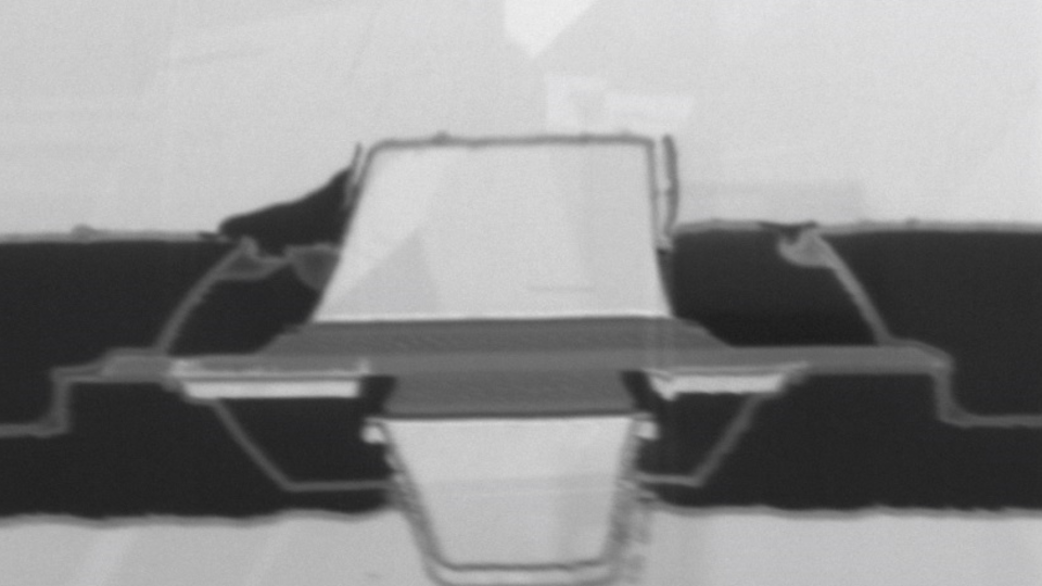
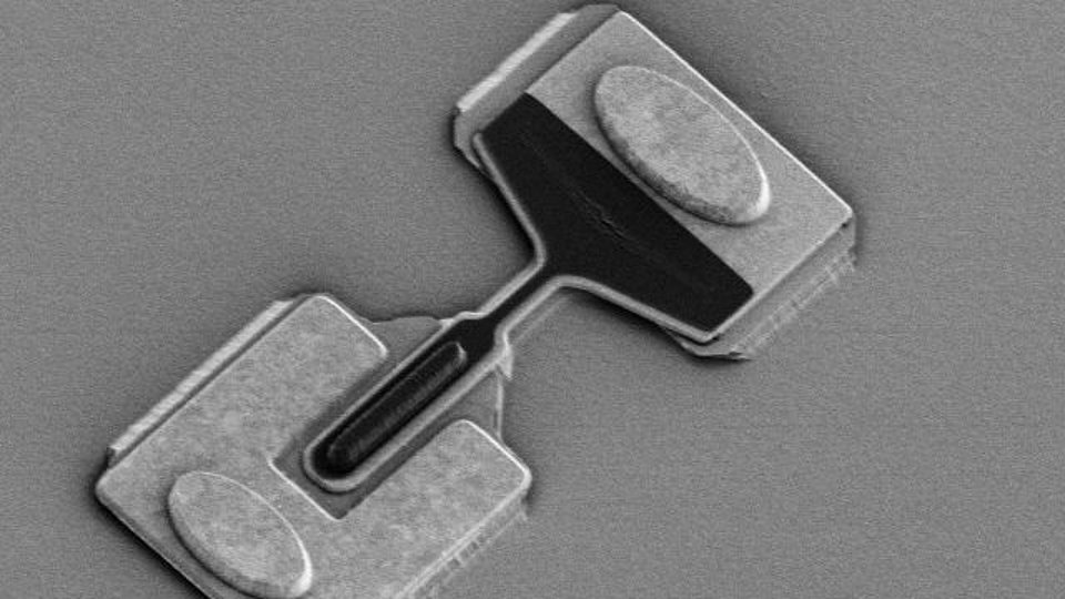
Using our transfer-substrate process, high-frequency integrated circuits are fabricated with InP heterobipolar transistors. The outstanding material properties of InP (high electron velocity combined with high breakdown field strength) can be optimally harnessed. Due to the adjusted lithographic access to the front and back side of the device, parasitic capacitances can be eliminated and a high frequency optimized circuit periphery can be realized.
For fast technology and circuit development, we offer a triple mesa topology. With cut-off frequencies > 200 GHz it is an important tool for prototyping and development.
-
InP HBT Technology for THz Applications
flyer (pdf)
