Digital Transmitters
Digitally driven, switched transistors are more and more THE core elements to push many areas of electronics to a new, higher level of development and thus make them future-proof. Fast and efficient switching enables the connection of power to high-frequency electronics (power meets RF). In fast power electronics (VHF range up to 300 MHz switching frequency), innovative circuit concepts play a decisive role in making power conversion for the supply of e.g. Point-of-Loads (PoL) in data centers for "Big Data" for processing the constantly increasing data volumes in the course of 5G more efficient. In the infrastructure of future mobile communications from sub-6 to 300 GHz (5G/6G) it provides more efficient power management capabilities and maximum flexibility as well as compactness. The target is the complete digitization of the components.
This paradigm shift significantly conserves resources and reduces CO2 emissions. Features that decisively advance the global project of green communication technology. Quantifying the energy saving potential of digitized transceivers for 5G networks below 6 GHz and making our unique measurement environment available to external customers has been pursued since mid-2022 in a sub-project (TP3, Hub2) of the BMBF project GreenICT @ FMD.
Especially this promising topic of energy consumption drives us and is our motivation with which we work on digital transmitters as a core topic for various fields in the Digital PA Lab.
Our topics focus on different applications from 100 MHz ... 300 GHz. In all cases, highly efficient high speed switching is required as a difference maker to push performances.
VHF DC/DC power converter
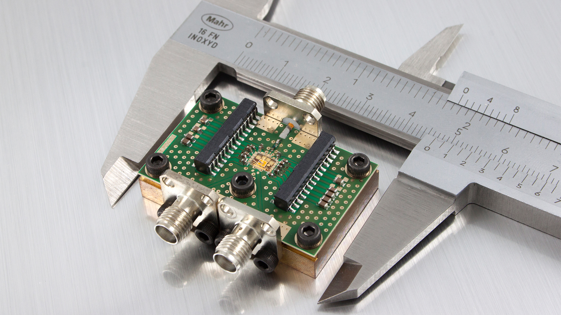
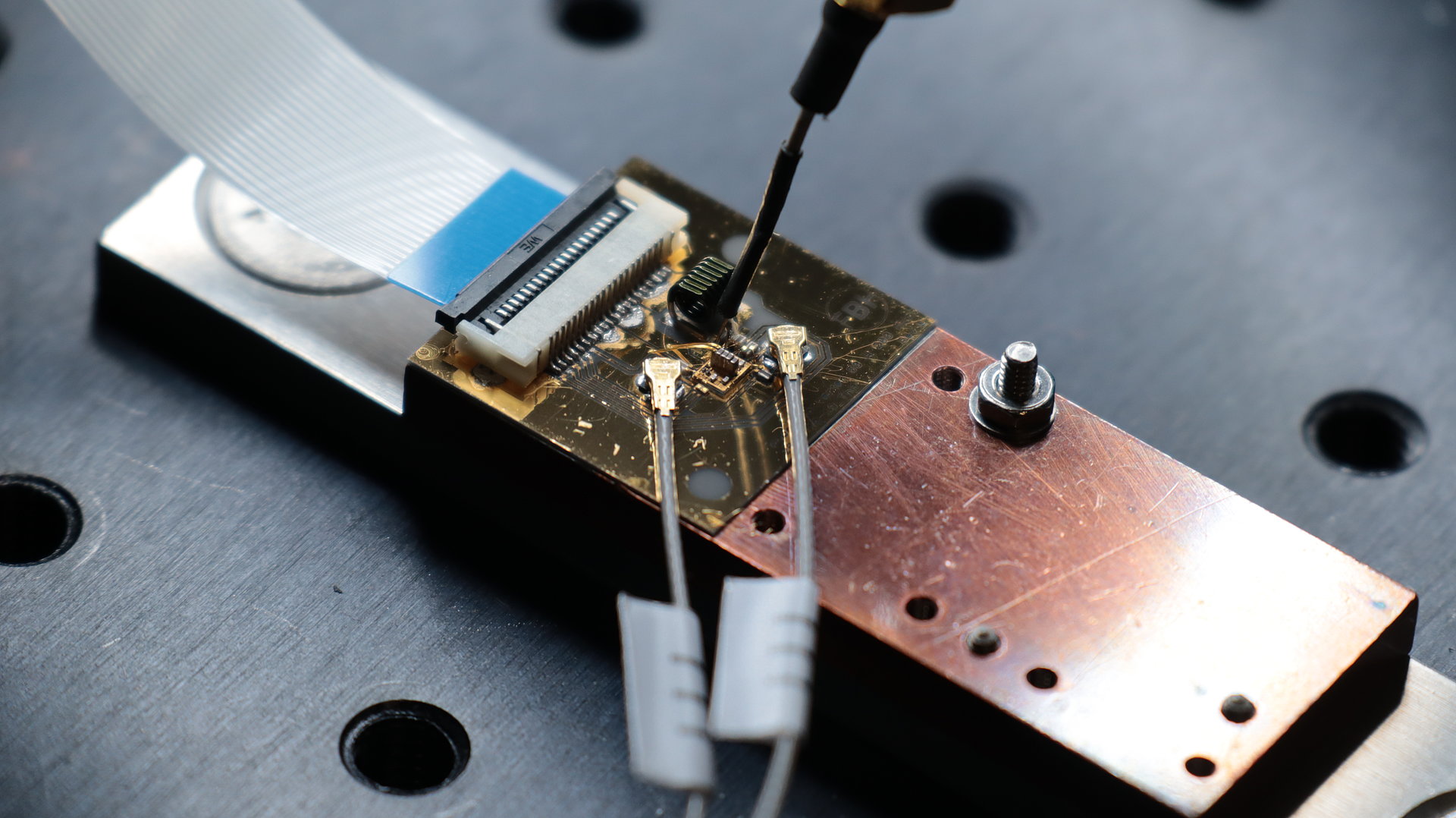
The demand for power electronics having greater compactness, better manufacturability, and higher performance has motivated a strong increase in switching frequencies to lower GHz-range. High frequency DC/DC converters can significantly reduce size of the passive components used for conversion output networks and energy storage. This leads to reduced form factor and weight, higher power density and faster transient response. Moreover, there is potential for monolithic integration of very compact supplies with greatly reduced parasitic inductances. Based on FBH 0.25 µm GaN prcoess we realize monolithic converter ICs with highly efficient gate drivers. They represent the core unit for different applications like buck converters for 48 V PoL energy conversion or supply modulators.
In addition, since 2022 AlN-based VHF power converters are designed in the DiPA Lab in the framework of the DFG Priority Programme 2312 "Energy Efficient Power Electronics ''GaNius'".
Digital PA modulator
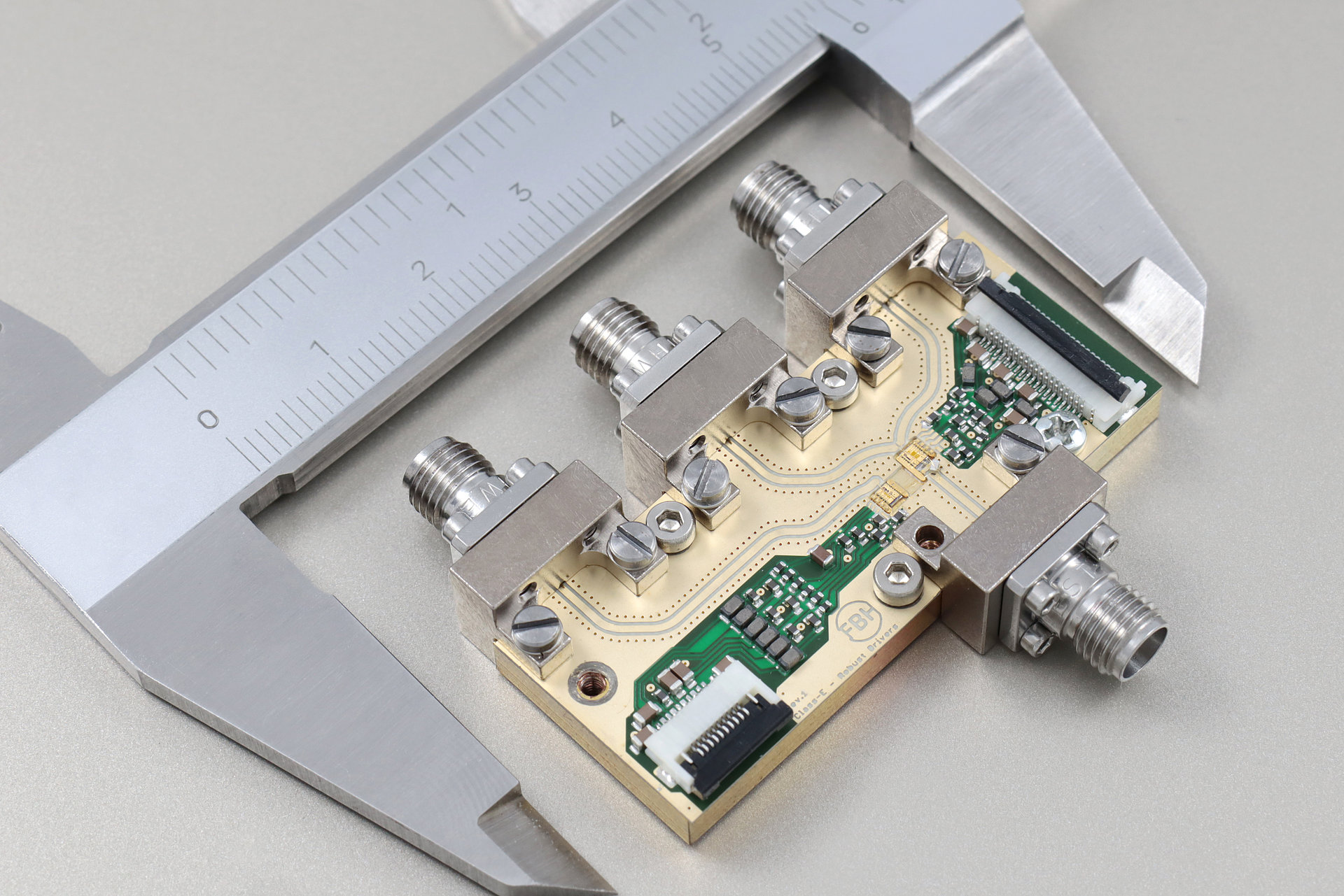
Patented digital modulator concept with highest linearity and integrated lossless DPD provides bit sequences perfectly tailored for digital switching PAs of any technology. Also, it can realize time delays with ps accuracy between several transmitter branches for phased arrays in digital beamforming networks.
To expand the application fields the modulator concept is planned to be implemented on CMOS in a joint effort with TU Berlin and represents together with an integrated PA a novel transmitter concept for more flexible, energy-saving handsets. This has been addressed in a 3-year DFG project since February 2023.
GaN-based digital transmitters
The GaN-based digital transmitter activities focus on sub-6 GHz MIMO systems with digital beamforming. This includes integration with highly robust LNAs to form digitized transceivers based mainly on strained GaN HEMTs. Varying the pinch-off voltage of the transistors should result in more efficient drivers and thus transmitters. In addition, the linearization capability inherent in the digital modulator allows the digital transmitter chains to be linearized according to the latest requirements without additional energy losses.
Besides the activities on the actual GaN-based digital amplifier part, there is another important block in the fully digital transmitter chain that we are working on:
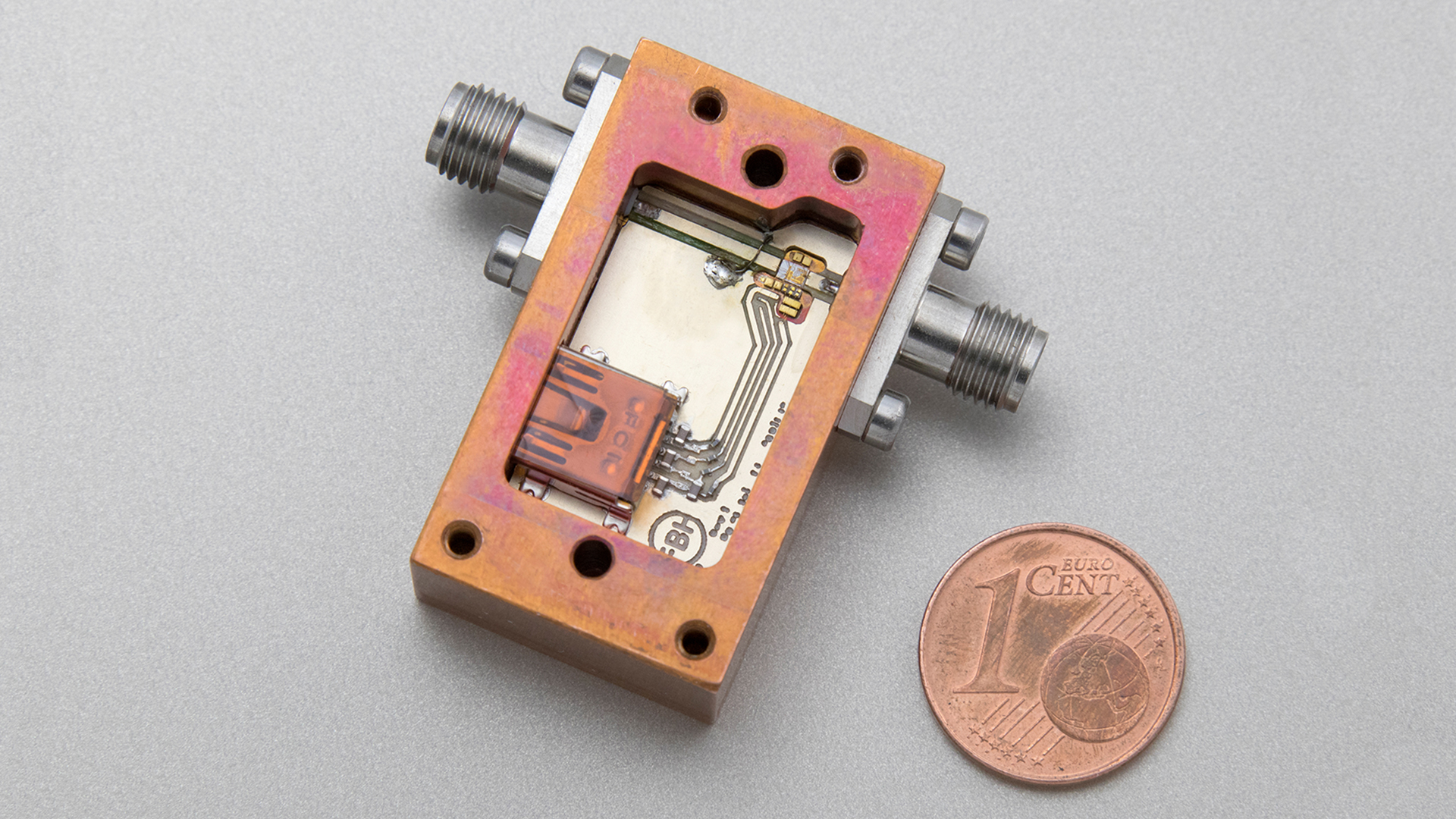
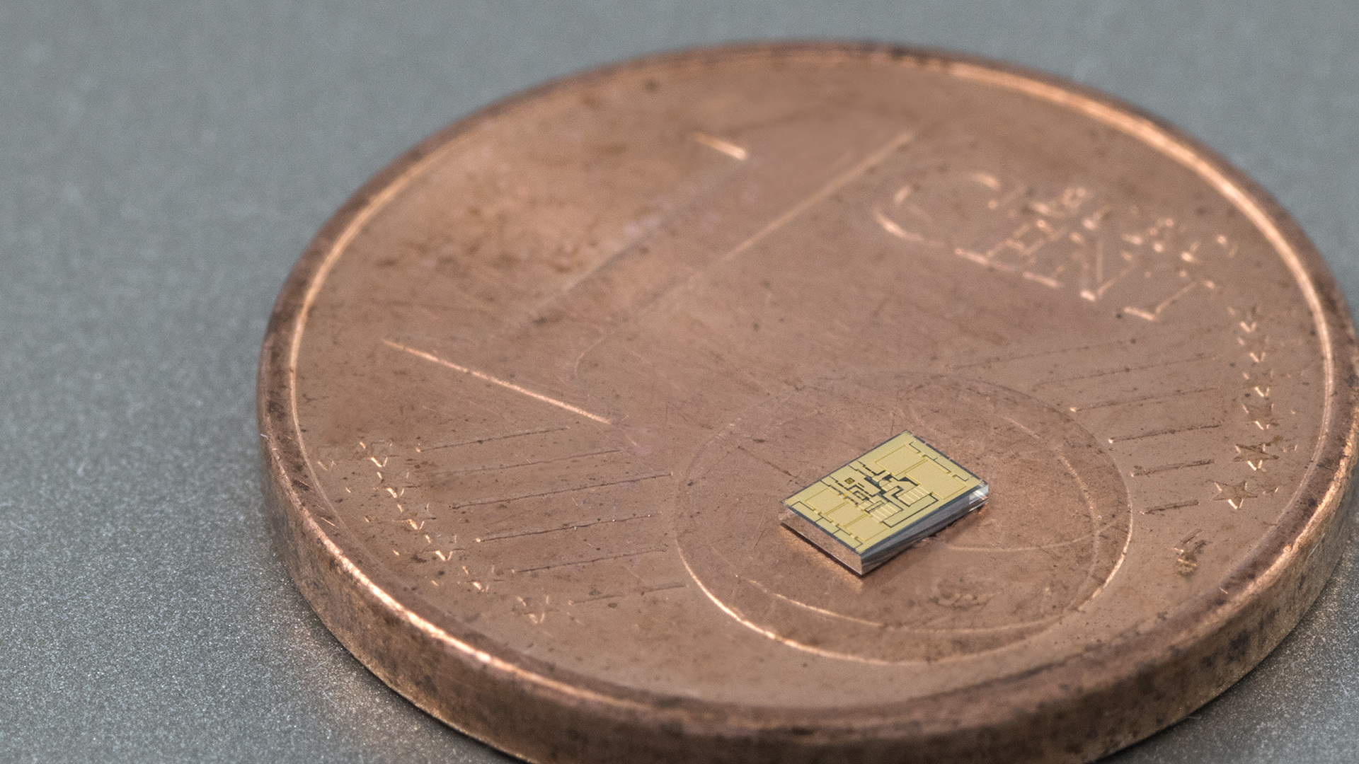
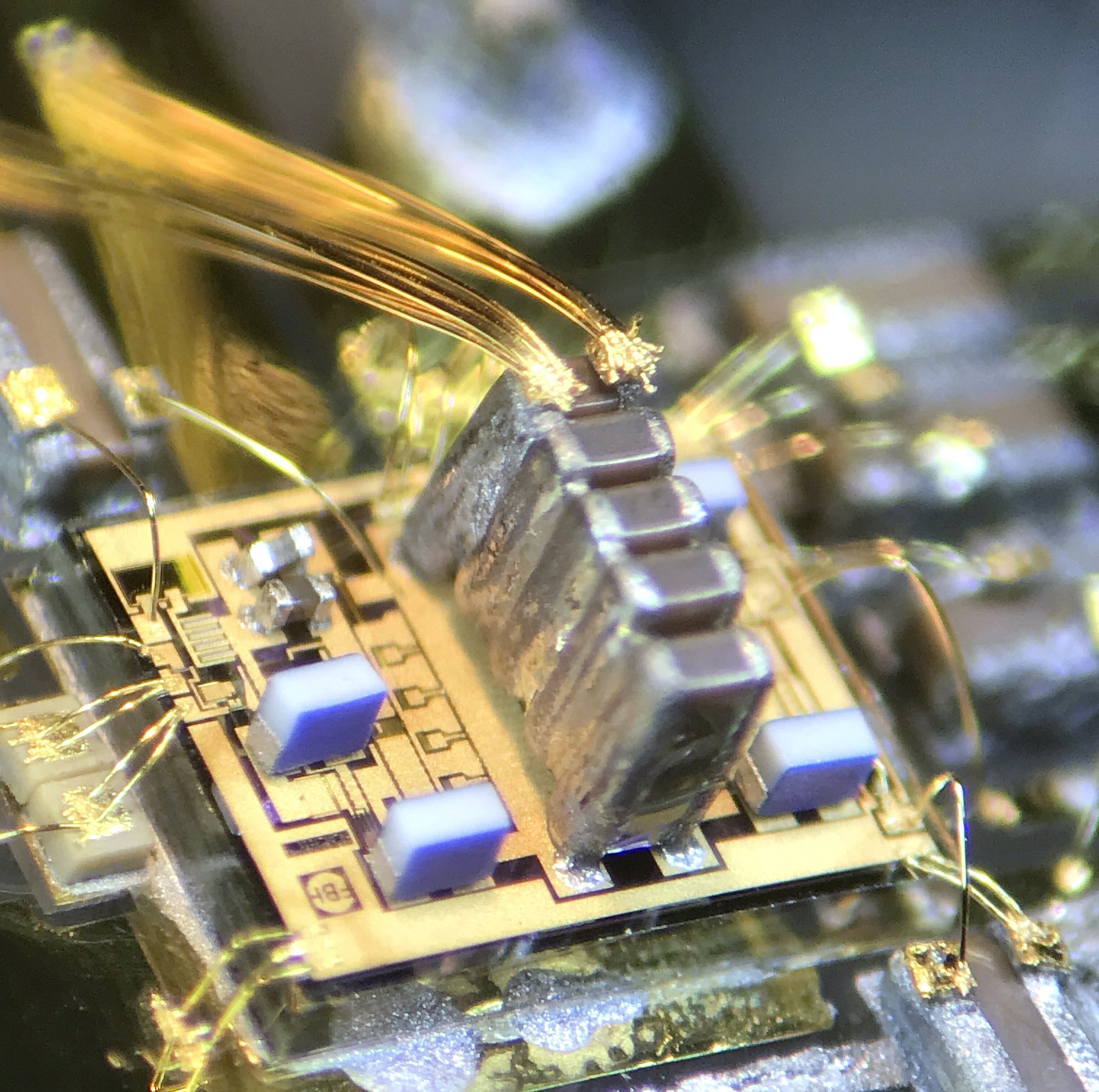
The otherwise common SiGe or BiCMOS digital pulse sources cannot directly drive GaN transistors digitally due to insufficient voltage amplitudes. In addition to 5 Vpp amplitude, DC-coupled digital and multistage GaN power amplifiers require a fixed DC potential at the input. This must be dynamically adaptable to different broadband input modulation schemes. A novel GaN-based driver amplifier module with integrated DC potential shifting meets all these requirements. The central element of the compact module is a GaN chip developed in the Digital PA Lab. The preamplifier provides a controllable shift between -1.5 V and -11 V. A voltage gain of 11 is furthermore achieved at a GaN HEMT typical input impedance. The 3 dB bandwidth is DC -3.2 GHz and the typical power consumption is 2.3 W.
In addition, a CMOS-based solution with extended breakdown voltage is also being worked on in parallel. This is being pursued in collaboration with the TU Berlin and the Mixed-Signal Circuit Design - Group of Prof. Friedel Gerfers.
Intelligent phased-array sub-THz transmitter and energy harvesting
We think Green ICT not only in the here and now, but already well ahead for 6G applications and beyond. Green ICT will also be a major focus in intelligent phased array sub-THz transmitters up to 300 GHz. Most efficient novel transmitter concepts with switching amplifiers are applied to the InP-based 6G circuits for wireless communications through intelligent designs at the limits of the technology. These highly efficient transmitters drive the green aspect of the massive scale arrays required for 6G. Interconnection with suitable high-speed SiGe technology based on 3D heterointegrated chiplets for more functionality is also planned.
Our roadmap in the sub-THz range is being expanded to include efficient rectifiers in InP technology for power generation in the context of the Internet-of-Things (IoT).
-
digital power amplifier

data sheet