Load & Supply Modulation

New solutions for RF power amplifiers must be efficient. The CO2 emission must be reduced but for information and telecommunication technology (ICT) the energy consumption increases. This is partly due to the introduction of higher frequency systems that fulfill our increasing need for higher data rates. Load and supply modulation are old concepts for efficiency enhancement that now find new applications to help us break this trend. They are particularly promising for wideband modulated power amplifier systems for modern telecommunication systems with large crest factor, i.e. large peak-to-average power ratio (PAPR). Such systems are developed and investigated in our RF Power Lab.

Power dissipation in power amplifier with fixed supply voltage (red)
Power dissipation in power amplifier with two-stage class-G modulation (red)

In supply modulation, the supply voltage for the amplifier is modulated with the instantaneous envelope of the signal. When the supply voltage continuously tracks the input envelope the concept is known as envelop tracking (ET). Another option that enables higher modulation bandwidths is to modulate the supply voltage in discrete steps. This in known as discrete level supply modulation (class-G).

At present, the work is mainly focusing on different types of envelope tracking (ET) systems. To make such systems efficient there are various challenges to cope with:

  • The modulator or DC/DC converter that provides the varying supply voltage has to deliver enough power at a very wide bandwidth efficiently. The overall efficiency of the system is the combination of the modulator efficiency and the power amplifier efficiency.
  • The RF-power transistors in the amplifiers need to be able to work efficiently and stable at various supply voltages. This requires development of novel transistors and measurement methods to properly characterize them in dynamic operation.
  • The RF-power amplifier needs to be optimized to work efficiently for a particular signal and supply modulation. RF and low frequency stability is important.
  • The supply-modulated system needs to meet the requirements of the specific standard and thus linearity needs to be improved using digital predistortion (DPD). Supply-modulated systems are more complex than conventional ones and require more complex models for the DPD to be successful.

An alternative method is load modulation where the load impedance of the amplifier is modulated with the envelope of the signal. 

The efficienzy of an amplifier at low output power can also be improved by changing the output impedans for the transistor. For high power amplifiers with large bandwidht signals this load tuning requires fast high power varactors with large tunability or fast switchable tuning stages. Such systems are alsu investigated for improved effizienzy and flexible reconfigurable power amplifier solutions. 

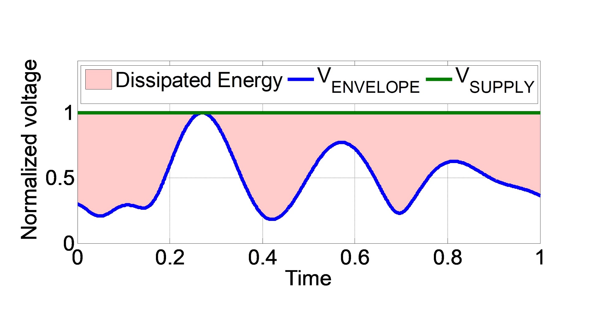
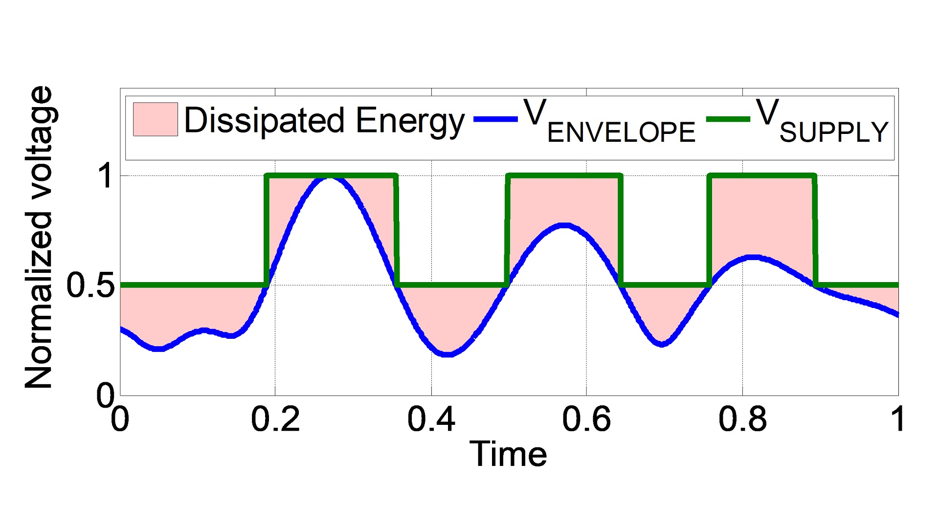
In general, the above-mentioned power amplifier systems are known as multiple-input systems. The modulated RF carrier accounts for one input and the control signal for the load or supply modulator as the second. Such systems with dual input and single output (DISO) enable flexible solutions for efficiency improvement at back-off output power but they require more efforts in design and modelling.  

Current research focus

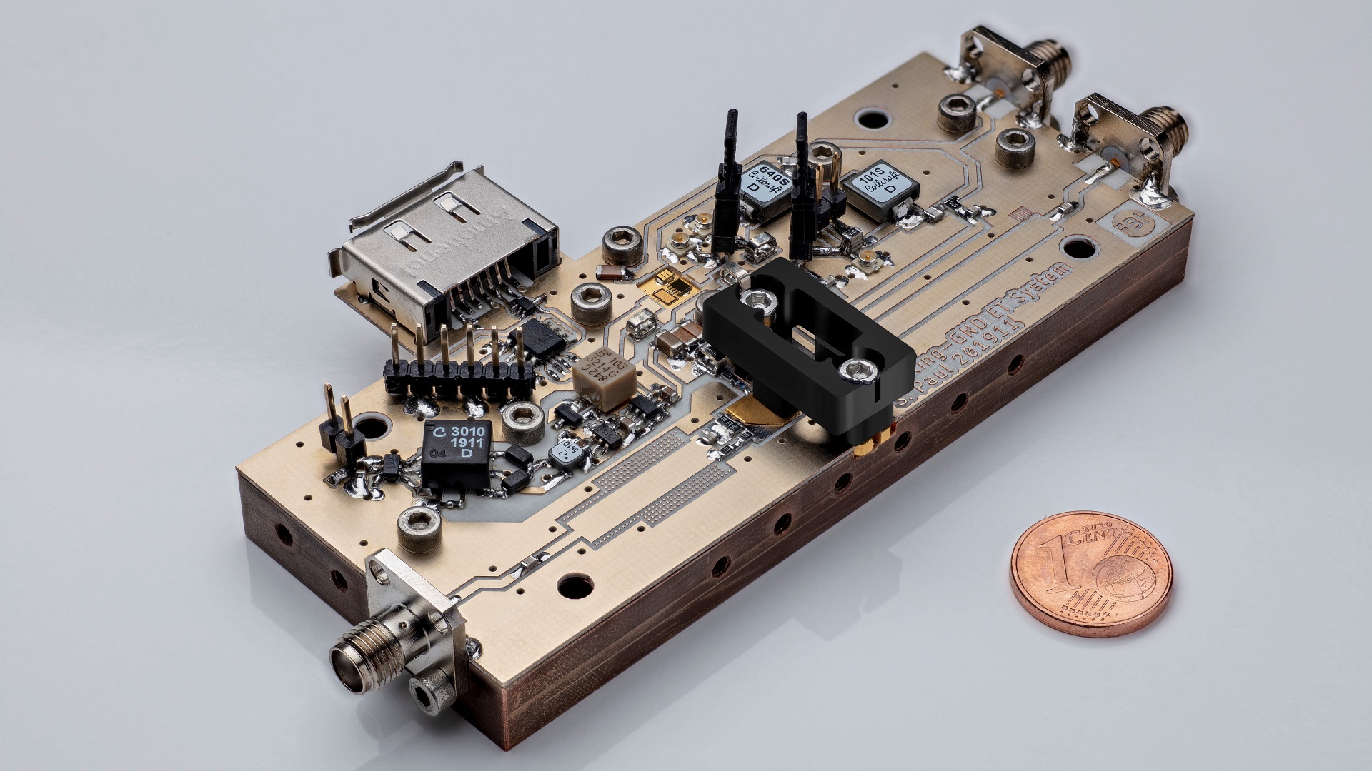
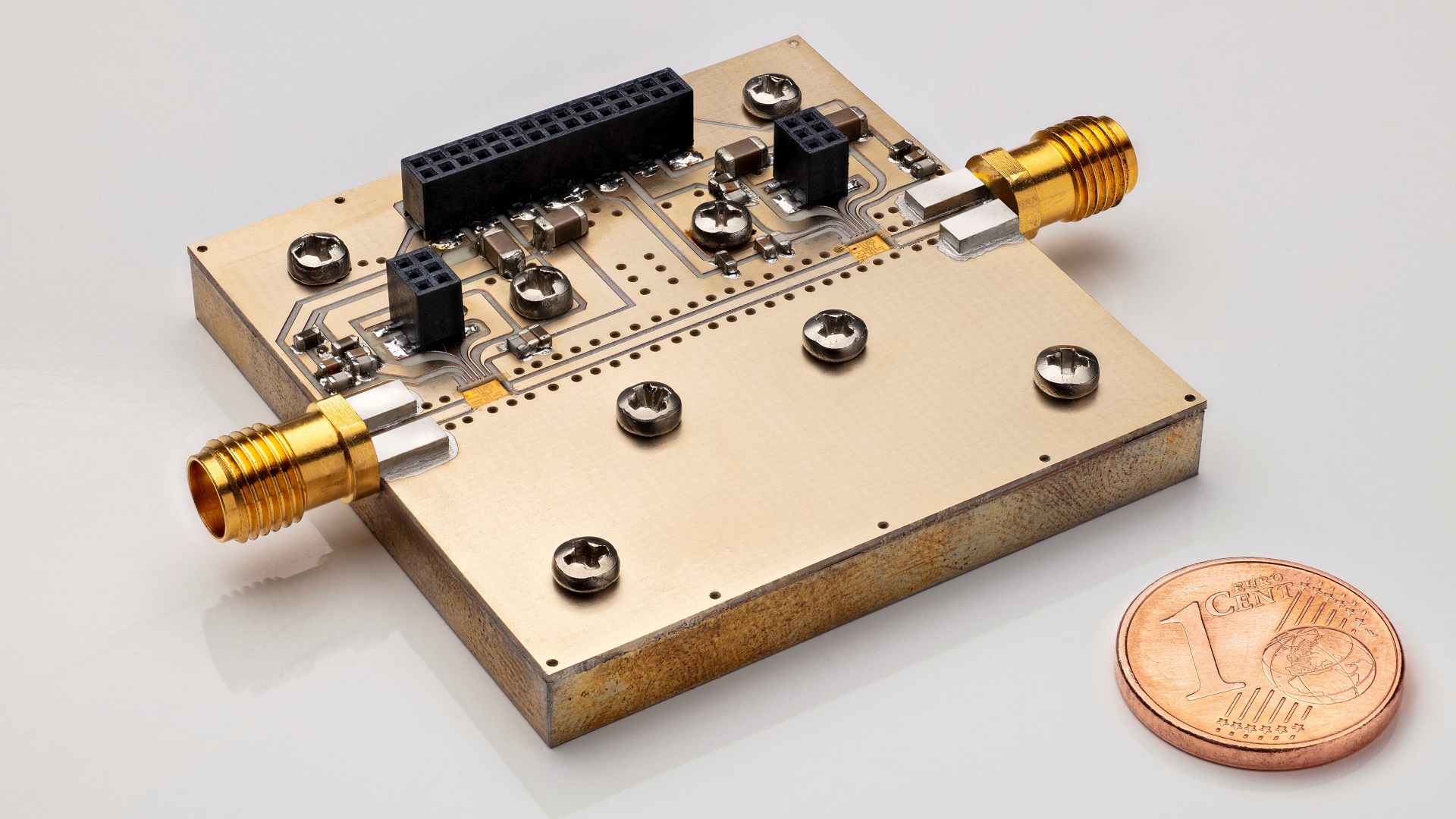
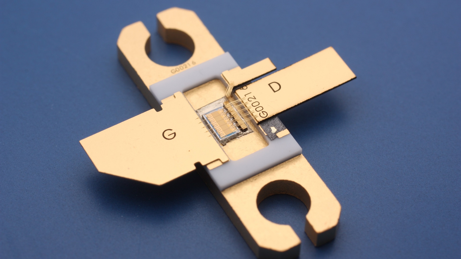
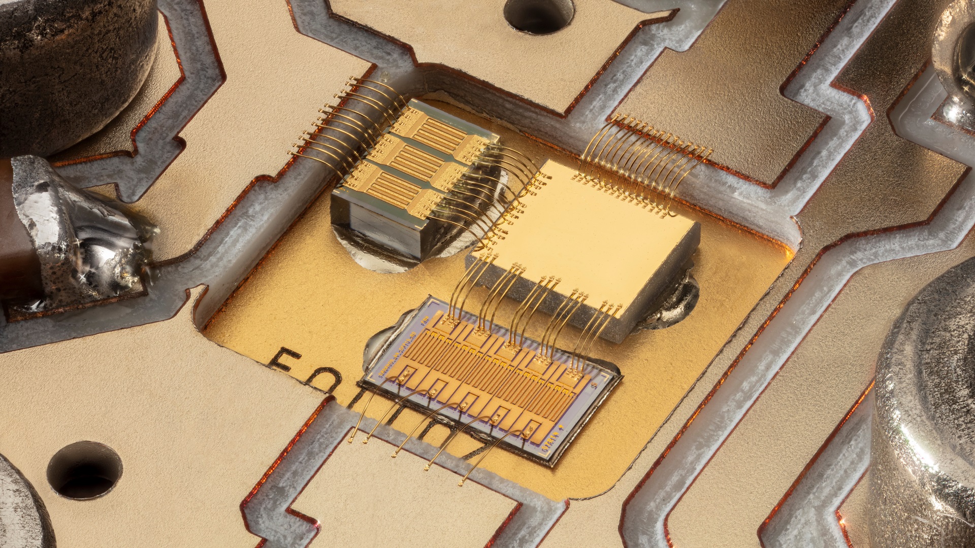
In the past we developed bread-board solutions for power applications ranging from 10 – 200 W in the RF frequency range below 6 GHz. In the past years we have changed focus and work mainly on MMIC solutions targeting efficient solutions for satellite communication in Ka-band (17 - 20 GHz) and for 5G-FR2 in the mmWave range (24 – 26 GHz) now.

The efficient MMIC power amplifier cells with output powers in the 10 W range are then combined as building-blocks for larger systems for beam-forming and MIMO.

In such large array systems, the RF power amplifier cells interact with each other. This cross-coupling is what we will investigate in the new 5G-MIMO measurements setup. In the future each power amplifier will be combined with a 3D integrated antenna to be measured over-the-air (OTA).

Systems & Applications

The aim of this project was to develop a 100 W discrete level supply modulated (class-G) GaN-based power amplifier system with 60 MHz instantaneous modulation bandwidth. It was a two-year project together with the University in Stuttgart financed by the German Research Foundation (Deutsche Forschungsgemeinschaft, DFG). The knowledge gained in this project is the foundation for the present work on integrated solutions for space and 5G applications.  

The class-G concept with discrete voltage levels in the supply modulation is now being implemented in integrated solutions for 5G and space applications. Multi-stage K-band integrated amplifiers are united on one chip with fast class-G switching cells. Alternative topologies are evaluated for efficient multi-amplifier systems for beamforming and MIMO.

In a reverse buck converter system, the converter is switching towards system ground and the RF power amplifier is operating at an offset potential. This kind of system offer a higher switching frequency in the modulator enabling a larger instantaneous modulation bandwidth. The goal of the project was to develop a GaN based 80 W RF power amplifier operating at 1.56 GHz based on a reverse buck converter topology. The system was initially implemented on bread-board with discrete packaged component but in a later version as a hybrid solution. The system offers about 10 MHz instantaneous modulation bandwidth with 45 MHz switching frequency. The two-year project was financed the European Space Agency (ESA) as a Networking / Partnering Initiative (NPI) cooperation. This project inspired the development of the floating ground transistor.

The patented floating ground transistor was developed to increase the instantaneous modulation bandwidth in envelope tracking systems based on reverse buck converters. Separating the RF ground from the DC-LF ground very close to the source on the transistor facilitates the amplifier design and enables a much higher cut-off frequency for the modulations bandwidth.

To facilitate the design of tunable RF power amplifiers we developed the tunable pre-matching transistor with a BST integrated in the package of the GaN-HEMT transistor. The concept was patented and successful implementations for Frequency agility and VSWR protections were presented. For load-modulation the varactors should to large losses to show benefits. Therefore, other concepts like GaN varactors, and switchable tuners that are also possible to integrate in the GaN process are now in focus of our work.

Together with the Technical University of Darmstadt (TUD) we have developed high power thick-film Barium-Strontium-Titanate (BST) varactors. They are targeting applications like load modulation and flexible frequency agile RF power solutions. They can handle more than 50 W in power but are still fairly lossy.   

Telecommunication systems are operating at higher and higher frequency to accommodate the need to transfer more and more information. The communication cells are getting smaller requiring less power to cover. Even so more and more applications in the lower frequency range with a need for high efficiency are evolving. Particularly in the free frequency bands for industrial, scientifically and medical (ISM) applications.

We are strongly involved in developing highly efficient solutions for these applications too. We work on RF Power GaN transistor technology but also generally on RF power amplifier design in kW range. Focus is research cooperation, master-works, and cooperation with companies and the RF Power Lab in high-power ISM applications.     

Transfer & Services

We offer development, evaluation, technical consulting and support in due-diligence in the field of load and supply modulation for flexible RF power systems for efficiency enhancement and frequency agility.

We work mainly in our own GaN technology but can offer our services on external processes as well if needed.

Selected Publications