Materials Analytics
Materials analytics plays an essential role in the development of epitaxial growth processes and in quality control for epitaxy and device fabrication. Due to fast and direct access to methods such as X-ray diffraction, photoluminescence, electroluminescence, carrier-density profiling, and electron microscopy, we are able to develop new epitaxial growth processes within a short time-scale. The rapid feed-back regarding the analysis of layer structures is indispensable for the production of highly complex devices (e. g. laser structures with integrated Bragg grating). Data from materials analytics are key informations for the quality management in epitaxy. Routine assessment of critical parameters after the exchange of source materials or maintenance of growth systems are the basis for our high quality standard products. The analysis of failure causes is essential for further device development and thus helps to push device technology forward. Our analytical methods and our expertise are also offered to partners and customers.
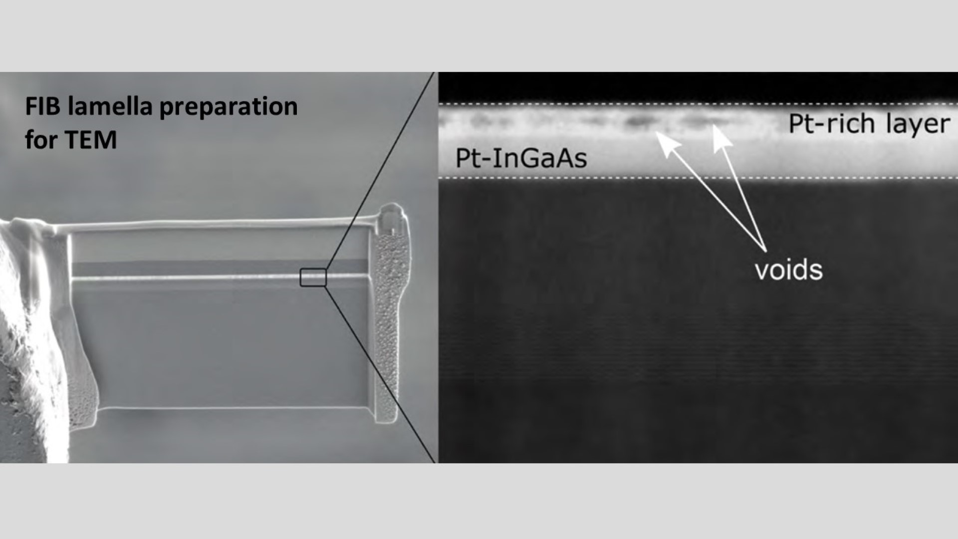
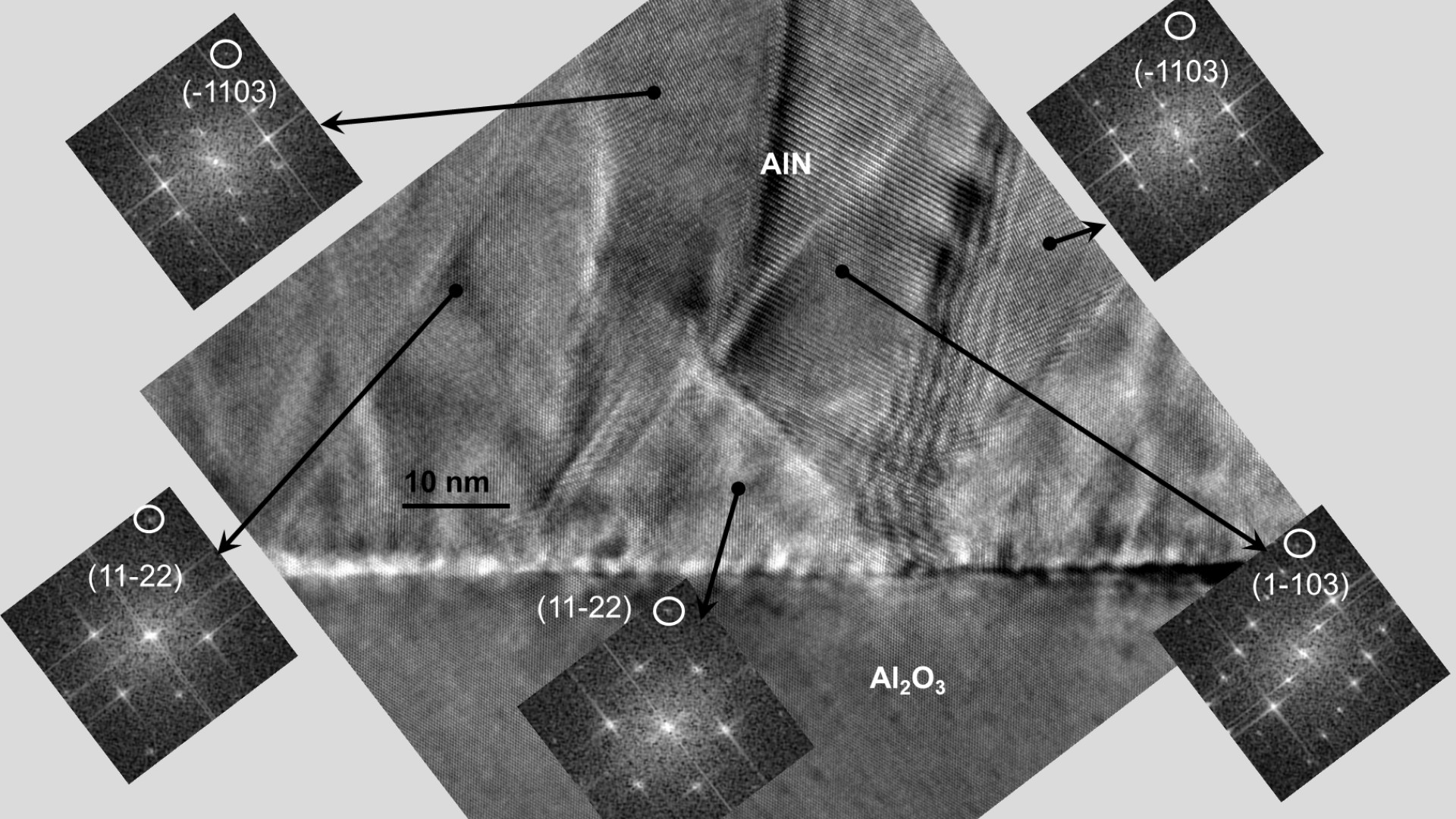
In-depth information on structural properties of semiconductor structures after certain epitaxial or process steps, in particular on the composition and design of interfaces on nanometer scales, is obtained via transmission electron microscopy (TEM). We use the instrumental equipment for TEM analyses within the framework of a partnership with the Humboldt-Universität zu Berlin.
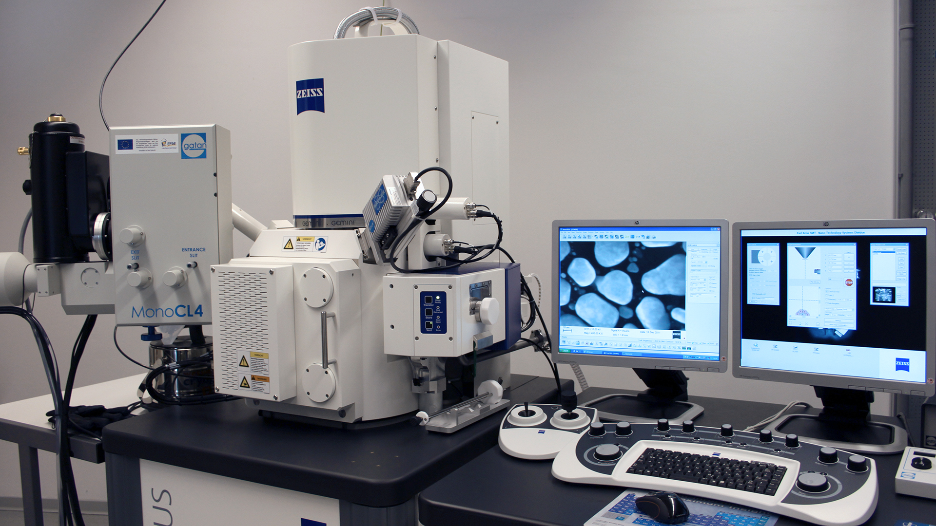
Electron microscopy
- Scanning electron microscopy (SEM) for surface analysis and measurement of layer thicknesses (high-resolution SEMs Hitachi S 4800 and Zeiss Ultra+)
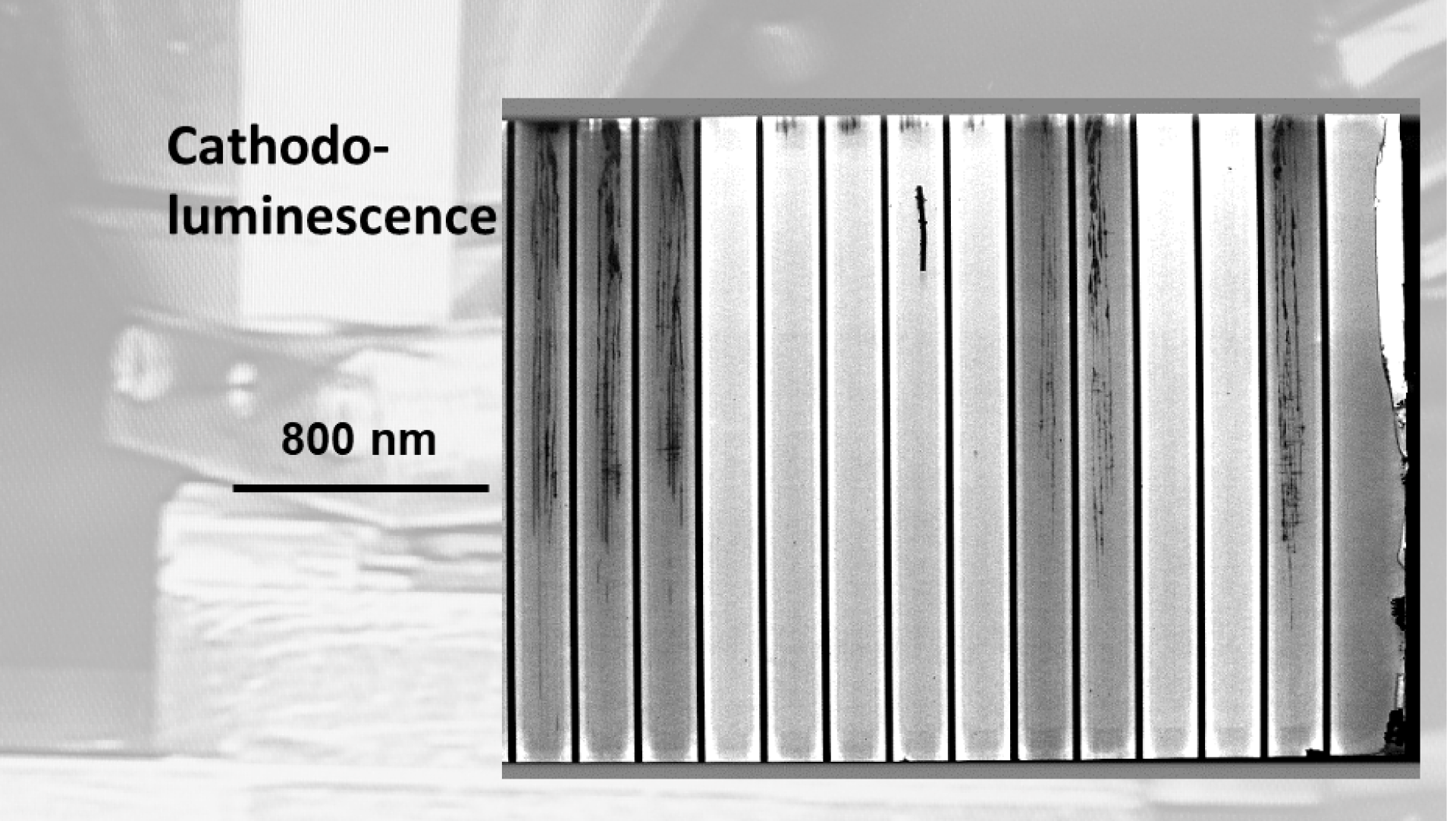
- Cathodoluminescence (CL) (T = 80 - 300 K) for spatially-resolved measurement of luminescence intensity and wavelength, measurement of spectrally-resolved mappings or linescans and for defect characterization and failure analysis (Zeiss Ultra+)
- Energy dispersive X-ray spectroscopy (EDXS) (electron microprobe) for local quantitative determination of compositions und for mappings of element distribution
- Sample preparation for SEM and TEM (cross section, plan-view preparation, FIB (focused ion beam) lamellae preparation)
- Analytic transmission electron microscopy (TEM) at HU Berlin for characterization of interfaces and defect structures, measurements of variations in composition or orientation on nanometer scales
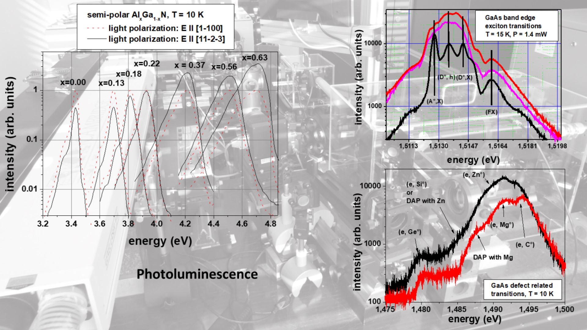
Luminescence analysis
- Room temperature photluminescence (PL) mapping for determination of emission wavelength and composition homogeneity (Laytec EPIX)
- Spectral reflectance mapping, transmittance and reflectance measurements for the determination of layer thickness (homogeneity), absorption edges, and DBR mirror characteristics (LayTec EPIX, Filmetrix F20)
- Low-temperature PL (T = 10 K) for analysis of material quality with excitation by laser wavelengths between 193 nm and 1020 nmand detection between 190 nm and 1700 nm
- Excitation power dependent and temperature dependent PL (T = 10 K - 300 K) for determination of internal quantum efficiency
- Electroluminescence (EL) for determination of spectral emission characteristics and P-U-I curves of LEDs and laser diodes
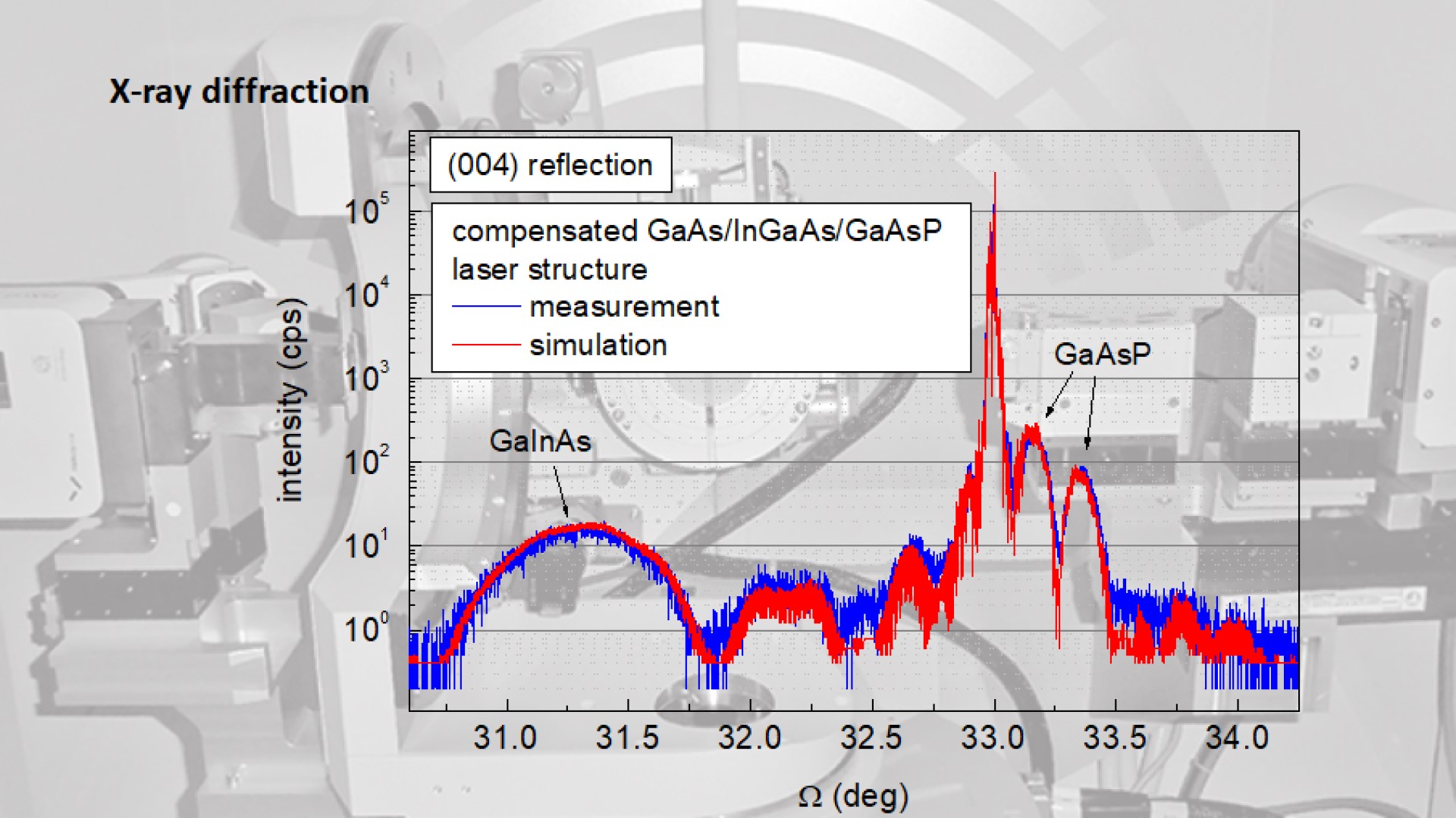
X-ray diffraction
High-resolution X-ray diffractometer for precise determination of composition, layer thickness and strain in single layers and layer stacks (PANalytical Xpert Pro and Xpert3)
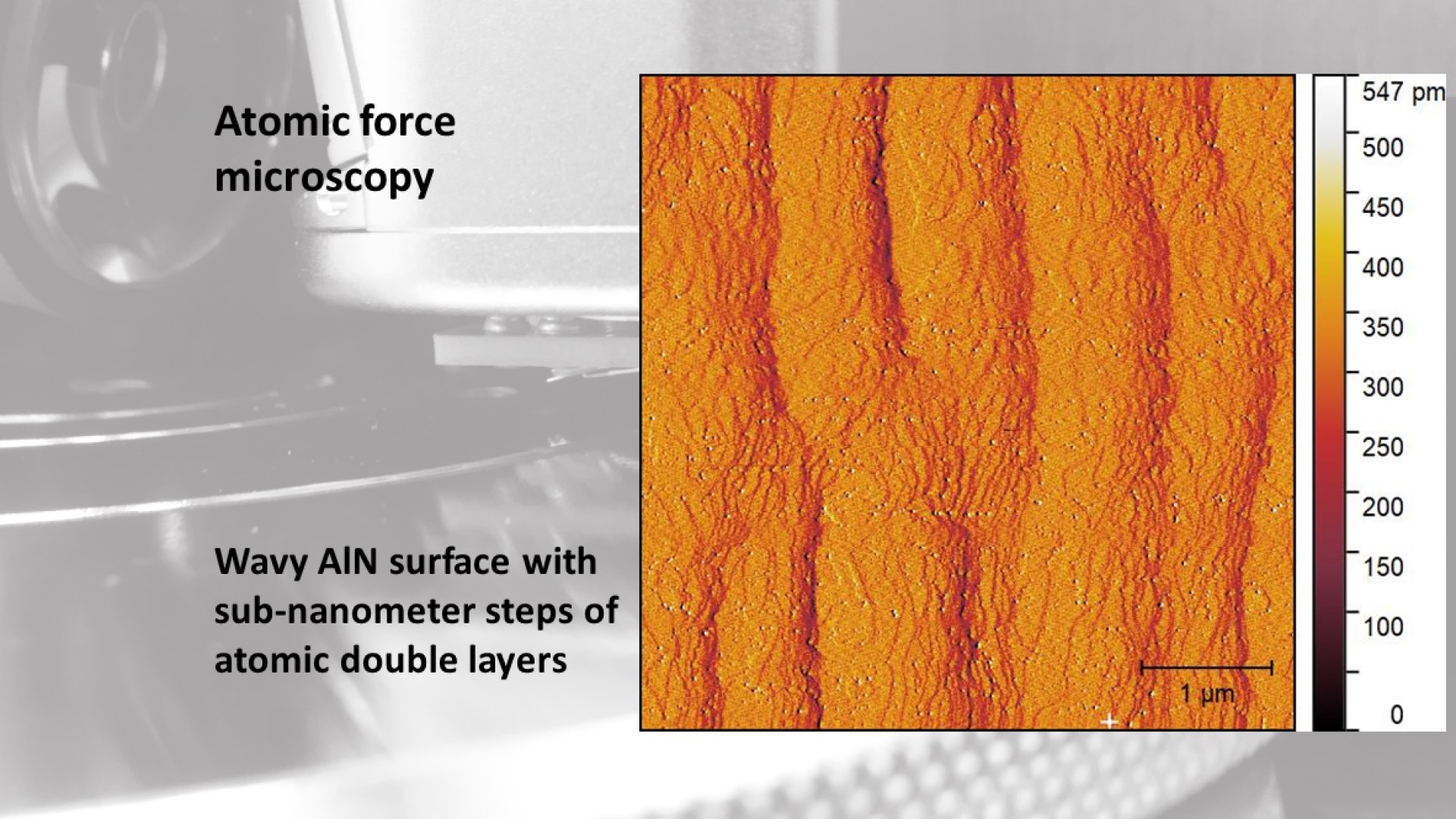
Atomic force microscopy
Atomic force microscopy (AFM) for surface roughness mappings and characterization of surface height structures (height resolution of about 0.2 nm) (Dimension edge from Bruker)
Carrier concentration
- Electro-chemical C-V-measurement of carrier concentration profiles (Accent ECV Pro, Accent PN 4300/4400, Dage CVP 21)
- Sheet resistance mapping (M-RES 2000M)
- Hall effect measurements for determination of carrier concentration and mobility (temperature dependent, magnetic field dependent)
Photocurrent
Spectrally- and time-resolved photocurrent measurements for photodiodes, in particular in the UV spectral range
We also offer our analytical processes and expertise as services to partners and customers: