Process Technology
Process Technology General Information
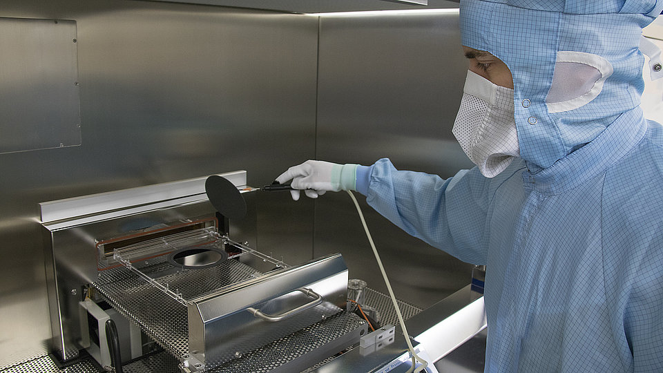
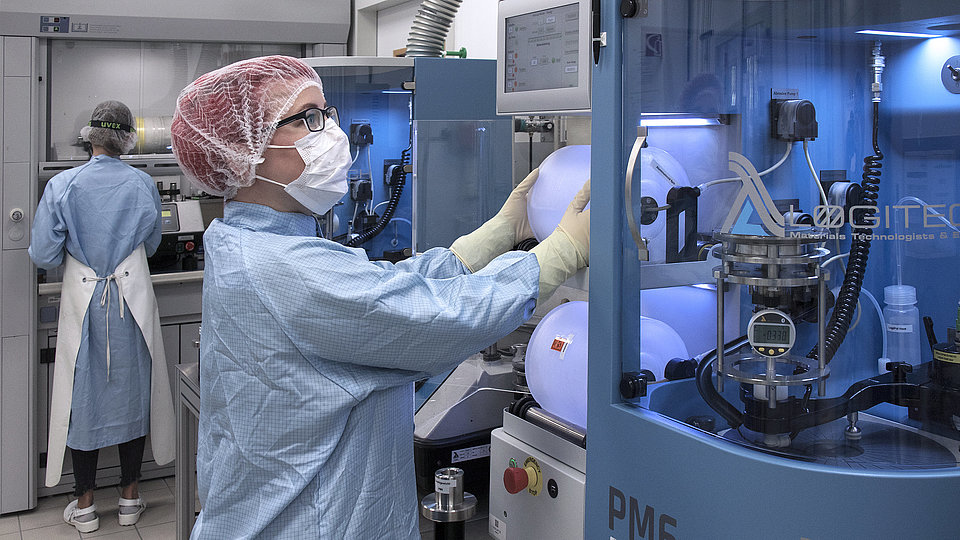
Wafers from 2" to 100 mm and different substrates (GaAs, InP, Si, SiC, sapphire, GaN) are processed in our cleanroom with high reproducibility.
With modern, industry-standard process equipment, we develop processes quickly, transfer them to small series if required, or transfer process modules to partners. The process line includes all technologies listed below for wafer patterning up to chip singulation.
Lithography
![[Translate to English:] Gate-Struktur mit Lithografie erzeugt](/fileadmin/_processed_/d/6/csm_SlantedGate_70nm_a4b2f3ac2d.jpg)
Photolithography
- up to 100 mm wafer diameter including special sizes and wafer parts
- i-Line exposure (365 nm) with stepper and mask aligner
- structure sizes up to minimum 350 nm
Electron Beam Lithography
- 2" - 100 mm wafer exposure with shape and spot beam systems
- 100 - 150 mm mask exposure
- 6 nm spot beam and 50 nm shape beam
Etching
![[Translate to English:] geätzte Struktur](/fileadmin/_processed_/e/a/csm_Fig2_v1_aa09cd9128.jpg)
Wet Chemical Etching
- manual and automated etching processes
- material selective etching with etch stop
- crystallographic etching
- selective undercutting
Dry Chemical Etching
- RIE- and ICP-based processes
- in-situ process control by laser interferometry
- established processes for semiconductors, dielectrics, metals and polymers
Deposition Process
![[Translate to English:] FBH Abscheideverfahren Reinraum [Translate to English:] Abscheideverfahren Reinraum](/fileadmin/_processed_/f/1/csm_KLEIN_MB_MB66593_BEA_09549f3ed8.jpg)
- PECVD deposition of insulators
- Electron beam deposition of various metals
- HF and DC sputtering processes for metals and dielectrics
- Electroplated gold deposition
Ionimplantation
![[Translate to English:] Ionenimplanter am Ferdinand-Braun-Institut](/fileadmin/_processed_/f/e/csm_FBH_Implanter_05_2021_tw_65112b846b.jpg)
- Medium current implantation system 15 keV to 500 keV
- Heatable chuck up to 800 °C
- Ions from gaseous
- Solid and liquid source materials
- Single and multiple
- Implantations
- Simulation of implantation profiles
Thermal Processes

Rapid Thermal Annealing (RTA)
- under N2, N2/O2 or Ar atmosphere up to 1100 °C
- under N2, Ar or forming gas atmosphere up to 1600 °C
Furnace Annealing
- under N2 or Ar atmosphere up to 800 °C
DC Process Measurement
![[Translate to English:] Messtechnik am Ferdinand-Braun-Institut](/fileadmin/_processed_/e/4/csm_KLEIN_MB_MB66996_BEA_5569f955df.jpg)
- inline PCM and TLM measurements on various wafer probers
- capacitance measurements in the range 1 kHz to 5 MHz (1 mHz resolution)
- probe cards with up to 18 pins
- measurement range: 10 fA to 1 A resp. 10 nV to 200 V
Thinning

- Lapping and polishing of GaAs, SiC, sapphire, GaN and silicon
- Wafer sizes of 2", 3" and 100 mm wafers as well as cuts
- Thickness homogeneity up to +/- 2 µm over a 100 mm wafer
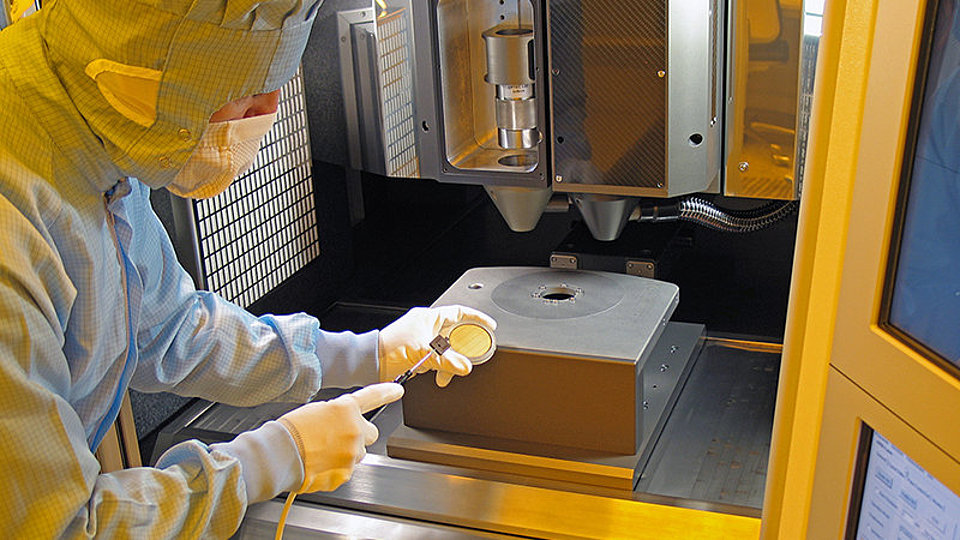
Sawing
![[Translate to English:] Sägen von Wafern und Waferteilstücken](/fileadmin/_processed_/e/e/csm_FBH_08_0005_Wafersaegen_601e2d2bf6.jpg)
- Sawing of e.g. GaAs, sapphire, SiC, Al2O3, Si, quartz glass
- Processing of 2" to 150 mm wafers as well as wafer parts
- Chips on foil in standard "ready for pick and place" sawing frame
Laser Microstructuring

- Micromachining with pulsed lasers
- Scribing, cutting, drilling of SiC, GaN, AlN, Si and sapphire
Process Accompanying Analytics
![[Translate to English:] Prozessbegleitende Analytik - Rasterelektronenmikroskop](/fileadmin/_processed_/9/6/csm_KLEIN_FBI_MB63135_BEA_7bf23f68f1.jpg)
- Ellipsometry
- Reflectometry (200 - 980 nm)
- X-ray fluorescence analysis (XRF)
- Energy dispersive X-ray spectroscopy (EDX)
- Scanning electron microscopy (SEM)
- White light interferometry
- Profilometry
- Defect density measurement
- Scanning acoustic microscopy (SAM)
- Atomic force microscopy (AFM, C-AFM)
We offer customized wafer processes and manufacture masks as well as reticles.
![Technology offer: Overview [Translate to English:] Technologieangebot des FBH](/fileadmin/_processed_/7/2/csm_Technologieangebot_FBH_2024_1432587108.png)