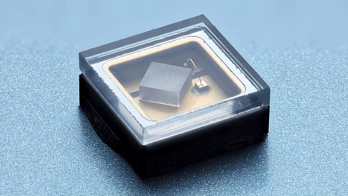
Mounting & Assembly
Many semiconductor chips such as high-power diode lasers and microwave-power transistors can only be fully characterized when mounted onto a heatsink or encapsulated. Chips that have been processed by the FBH are thus assembled in the Mounting and Assembly Department (AVT). Subsequently, they are passed on to the III-V-Electronics Labs, the Photonics Labs and Integrated Quantum Technology for characterization and lifetime testing or are delivered to customers and partners.
The AVT laboratories for mounting of semiconductor chips occupy more than 150 sqm of cleanroom space at the FBH, featuring manual and automated work stations as well as equipment for controlling and inspection to complete the following technology steps:
Die-Bonding
- flux free bonding of lead-free solders (AuSn, SAC, In) under forming gas-, formic acid- and hydrogen-atmosphere
- automated dispensing and gluing of thermal and eletric conductive/non-conductive adhesives
- sintering of nano-silver pastes
Flip-Chip-Bonding
- flux free bonding of lead-free solders (AuSn, SAC, In) under forming gas-, formic acid- and hydrogen-atmosphere
- thermocompression of gold-(micro)-studs
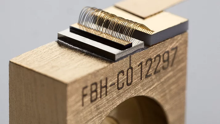
Wire- and ribbon-bonding
- 17,5 µm and 25 µm gold thin wire bonding in wedge-wedge- or ball-wedge-technology
- 100 x 20 µm gold ribbon bonding