Image Service
Please respect the copyright when using our pictures. The images on this website are intended for press purposes and may not be used commercially. Publication is only permitted in an editorial context and within media coverage about the FBH. Printing or publication is free of charge if the source and, if indicated, the photographer are mentioned.
We appreciate a brief notification about the usage of our images.
Images related to press releases
can be found directly on the page of the respective release
-
Logo
Logo (jpg, rgb modus) of Ferdinand-Braun-Institut, Leibniz-Institut für Höchstfrequenztechnik. Please contact our public relations office in case you need further formats.
-
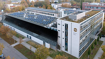
Aerial Image of the Ferdinand-Braun-Institut
© FBH/Christoph Ruß
Aerial view of the Ferdinand-Braun-Institut – main building. In the foreground, with the FBH logo, is the extension building opened in 2015) with laboratory and office spaces. To the left is the rear facade of cleanroom-1, which is clad with solar modules. The entrance to the main building is on the side not visible in the photo.
-
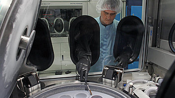
Metal Organic Vapor Phase Epitaxy (MOVPE) - Planetary Reactor
© FBH/P. Immerz
Multi-wafer reactor for Metal Organic Vapor Phase Epitaxy (MOVPE) of gallium nitride. Substrate wafers are put inside a sluice and seperately placed into the reactor. During this first step on its way to the final device atomic-thin layers are deposited onto the substrate material (= wafer).
-
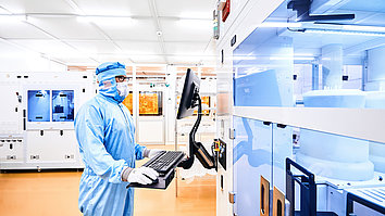
Electroplating System in the Cleanroom of the Ferdinand-Braun-Institut
© FBH/Matthias Baumbach
Electroplating – this electrochemical process is used to apply metallic layers to semiconductor wafers. Areas of the wafers that have been covered beforehand, e.g. with photoresist, are not electroplated. This allows precise control over where the electroplated layers are formed on the wafer and enables structures in the micrometer range and below to be produced.
-
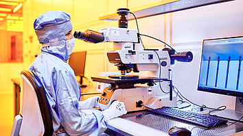
Microtechnologist in the Cleanroom
© FBH/ Matthias Baumbach
Microtechnologist at the microscope during wafer inspection
-
On-wafer Microwave Measurement
© FBH/schurian.com
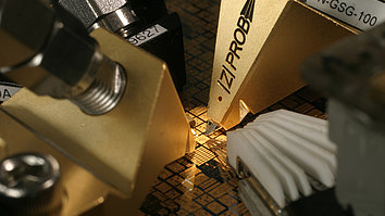
Measurement of single circuits with special probe tips, which only insignificantly distort the RF properties of the circuits. The distance of the contacts is usually in the range of only 50-150 micrometer.
-
Electroluminescence Measurement of AlGaN UV LEDs Using a Wafer Mapper
©FBH/schurian.com
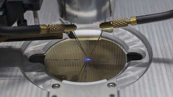
This wafer mapper is used to determine the characteristic properties of AlGaN-based UV LEDs on a 2-inch wafer such as optical power, voltage, and wavelength and to investigate their uniformity. The UV radiation of these LEDs is used, among others, for medical applications in dermatology, for sensing, and disinfection.
-
Wafer with Terahertz Circuits
©FBH/schurian.com
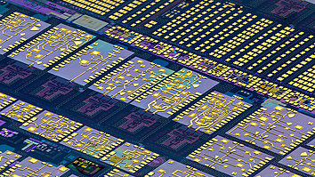
Terahertz (THz) circuits in InP-on-BiCMOS technology for THz signal generation. The high-frequency indium phosphide (InP) double-heteorostructure bipolar transistors (DHBT) are heterointegrated onto a silicon BiCMOS wafer. The dark areas indicate BiCMOS oscillators at 82 GHz and the brighter circuit parts are InP-DHBT multipliers and amplifier circuits.
-
Wafer with Laser Diodes
© FBH/schurian.com
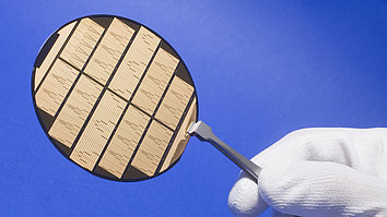
Completely processed 3" wafer with laser diodes.
-
UV Light-Emitting Diode (LED)
© FBH/schurian.com
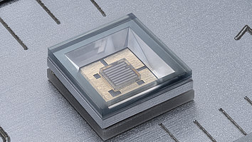
AlGaN-based UV LED chip mounted in flip-chip geometry in a hermetically sealed AlN ceramic package with a quartz lid. The package protects the chip in humid environments and efficiently dissipates the heat. The UV light emitted by the LED can be used for plant growth lighting, dermatology, sensing, disinfection, and others
-
Pump Laser Modules
© FBH/schurian.com
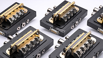
Kilowatt-class pump laser modules for high-power laser applications
-
Compact Fiber Coupled Amplifier Module
©FBH/schurian.com
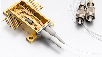
Fiber coupled amplifier module with emission in the yellow spectral range with integrated frequency conversion to the yellow spectral range at 561 nm with 200 mW for biophotonics applications.
-
Quantum Light Module for Use in Medicine & Life Sciences
© FBH/schurian.com
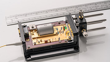
Quantum light module for optical coherence tomography (OCT) and spectroscopy measurements in the mid-infrared (MIR) range using “undetected photons.” The FBH quantum light modules are based on entangled photon pairs that are brought to interference in a nonlinear interferometer, thereby making the MIR spectral range accessible. Measurements are taken entirely in the more cost-effective near-infrared (NIR) range.
-
High-Power Pulsed Nanosecond Laser Sources for ToF LiDAR
© FBH/P. Immerz
High-current nanosecond laser driver with integrated ridge-waveguide laser diode for LiDAR applications. The FBH provides grating-stabilized diode lasers with multiple epitaxially stacked active regions that are suitable for pulsed nanosecond operation in time-of-flight (ToF) LiDAR. These are used, for example, to measure distances in the automotive sector.
-
GaN/AlN half-bridge chip with integrated drivers
© FBH/P. Immerz
GaN/AlN-based 2x120 mOhm half-bridge chip with integrated gate drivers for kW-range power conversion up to 400 V. The particularly low parasitic inductances and intrinsic switching losses of this power IC target efficient power conversion up to 2 MHz switching frequency. This allows for small and light-weight power converters with high power density. -
Digital Power Amplifier Module for Modern 5G Mobile Communications
© FBH/schurian.com
The novel module can be flexibly used for different frequencies, is very compact, and highly efficient. These features make it particularly attractive with respect to the digitalization of base stations for mobile communications since the power amplifier mainly determines the efficiency of the overall system and thus operational costs.
