Arsenides & Phosphides Epitaxy
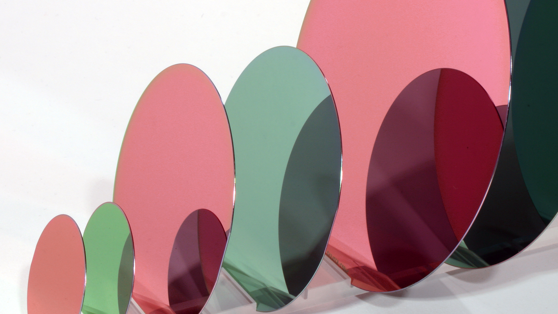
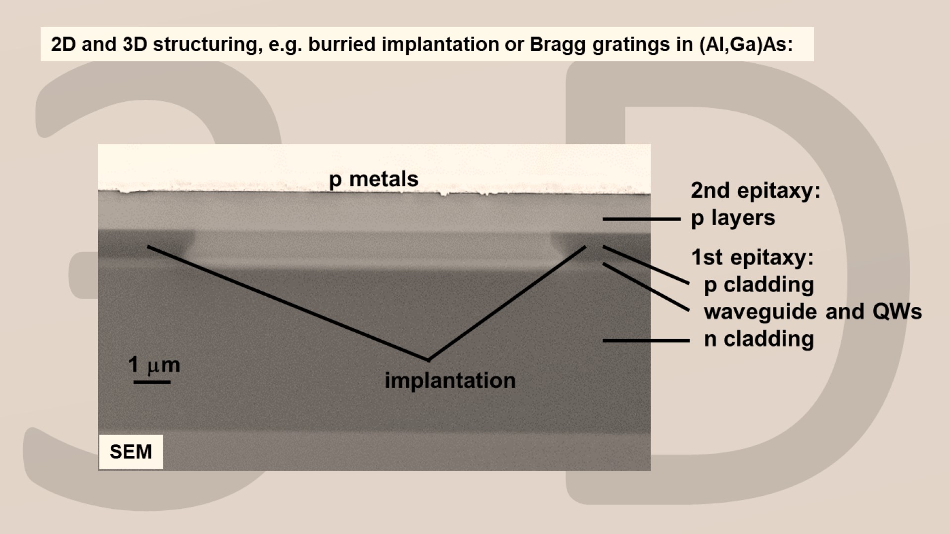
The deposition of single-crystalline compound semiconductor layers (epitaxy) with well-defined optical and electrical properties is the basis for GaAs- and InP-based microelectronics and optoelectronics. In the field of arsenides & phosphides, we develop semiconductor layers for optoelectronics in the range between 620 nm and 1200 nm for high-power laser diodes with excellent beam quality. Using two-step growth processes, we fabricate structures with gratings for wavelength stabilization or with burried implantation for current apertures. In cooperation with customers, we also develop saturable absorber structures for use in pulsed laser systems and in gain structures for vertical-external-cavity surface-emitting-lasers (VECSEL). Likewise, we develop vertical-cavity surface-emitting laser (VCSEL) with customer-specific properties.
Our continuous development and optimization of deposition processes for the material systems (Al,Ga)As, (Ga,In)(As,P), and (Al,Ga,In)P warrants the required high layer and interface qualities as well as accurate composition and doping. We supply epitaxial structures for internal use as well as for external partners and customers.
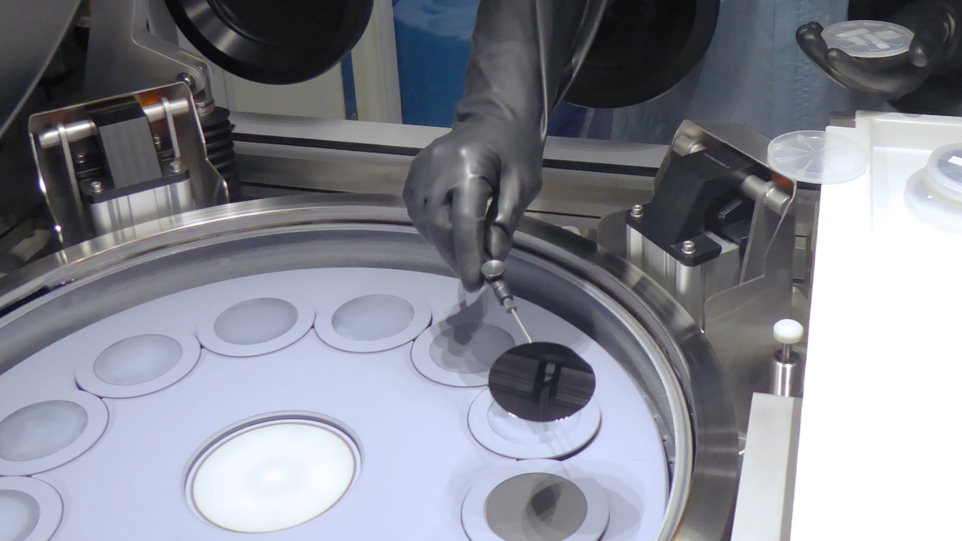
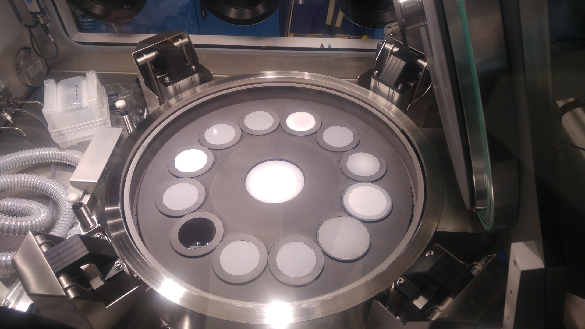
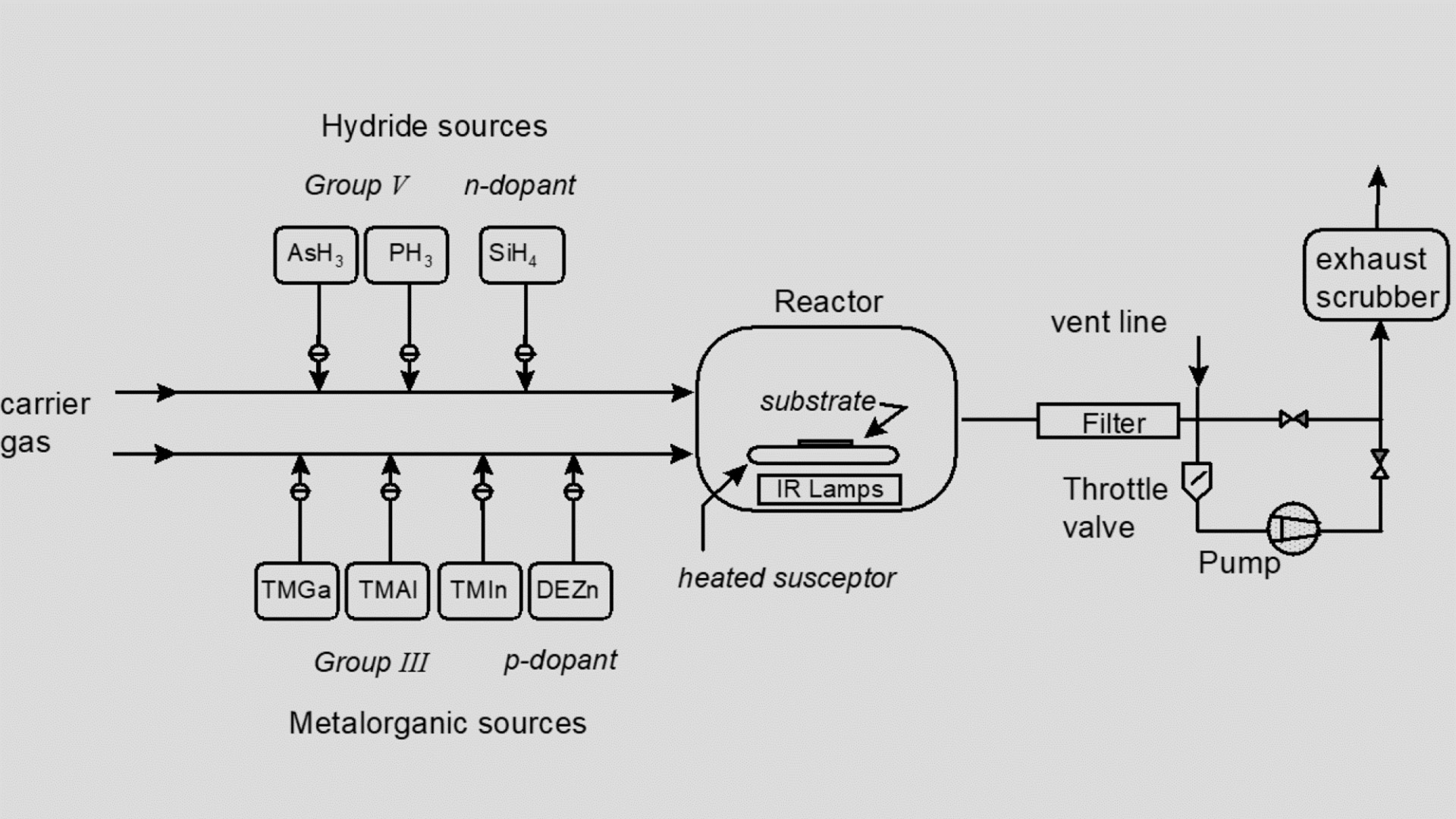
We use metalorganic vapor phase epitaxy (MOVPE) as growth process with TMGa, TEGa, TMIn, TMAl, arsine, phosphine, disilane, DETe, DMZn, Cp2Mg and CBr4 as sources. An accurate control of the purity of these starting materials is essential for the high quality of our layer structures. We use two identical reactors of the tpye AIX 2800G4 (12×4"), compatible with industrial standards, for layer production.
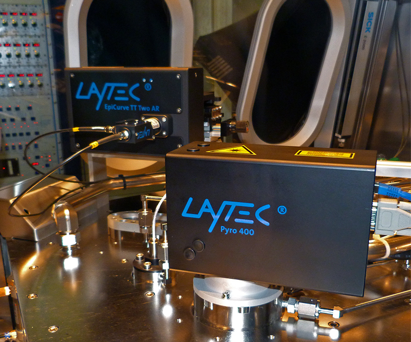
The MOVPE systems are equipped with in-situ tools for optical growth control by reflectance spectroscopy. These tools allow for fast development of epitaxy processes, a fast transfer of processes between different growth systems and a monitoring of processes over many years. We closely cooperate with LayTec AG on the development of these in-situ techniques.
For our customers we realize semiconductor layers with defined optical and electrical properties:

