Lateral GaN Transistors & Half Bridges
Lateral GaN-based transistors (AlGaN/GaN HEMTs) use a two-dimensional electron gas (2DEG) as transistor channel. They enable efficient power converters with particularly high power density. Very high converter switching frequencies can be realized because of the low area-specific on-state resistance (for a given off-state voltage) and the very low gate charge which is required for switching. This allows for very compact power converters. The lateral device design opens the path for straight-forward monolithic integrationn of the needed powerelectronic functionalities on one chip.

Normally-off 600 V GaN transistors with p-GaN gate
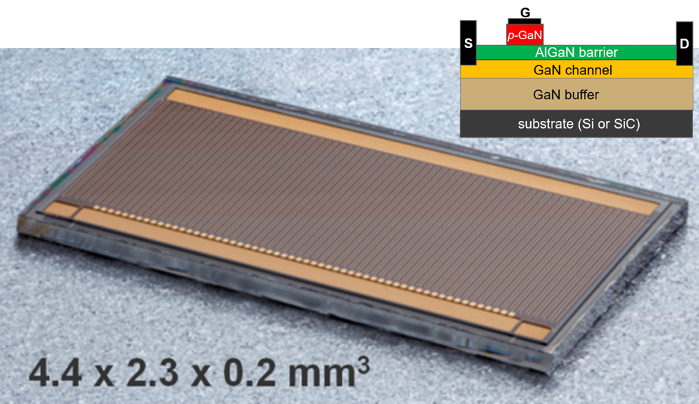
Chip photo of a self-locking 600 V/60 mOhm GaN switching transistor and its schematic structure
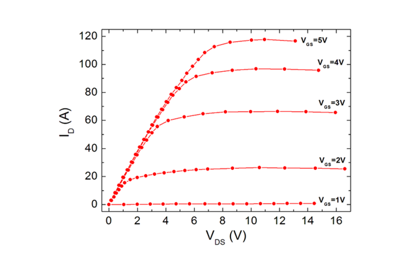
Output characteristics of a 600 V/60 mOhm GaN normally-off switching transistor
We use an own device process for 4" GaN-on-SiC or GaN-on-Si epi-wafers to manufacture lateral normally-off GaN transistors with up to 650 V blocking voltage.
Our p-GaN gate module converts the GaN-HEMT transistor with initially normally-on properties into an intrinsic normally-off device with positive turn-on voltage. Normally-off devices are needed for inherently safe power electronics.
Our 600 V switching transistors with 60 mOhm on-state resistance deliver a maximum pulse current of more than 100 Amps and are designed to operate in kilowatt-range power converters. The device capacitances and in particular the gate charge are significantly reduced with respect to conventional silicon-based power switches of the same rating. Switching transients in double pulse environments with inductive load show high voltage and current gradients and enable particularly short switching times with low switching losses.
Monolithic GaN half bridges
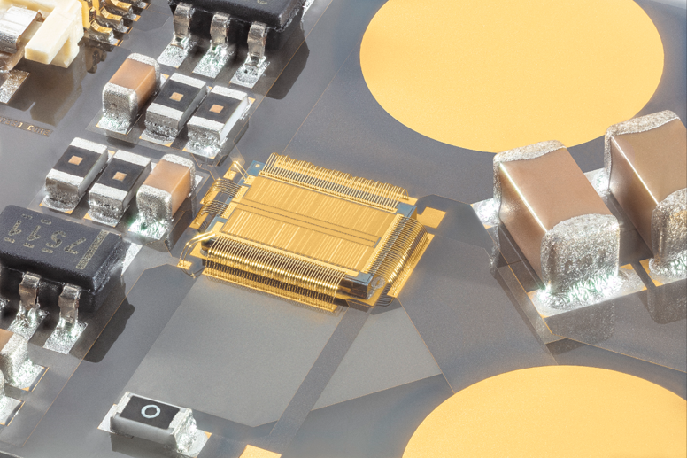
Monolithically integrated 170 mOhm/600 V GaN half-bridge chip in a low-inductance converter structure
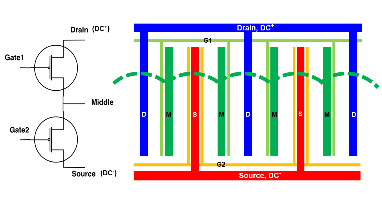
In an interleaved half bridge, the upper and lower switching transistors are already adjacent to each other at the source and drain finger level
We realize monolithically integrated half bridges that are based on our p-GaN gate normally-off GaN transistor technology.
High-side and low-side power switches of a half-bridge module can be integrated on one die since source, gate and drain terminals are all accessible on the chip surface. This enables particularly small power commutation loops of a power converter cell, which is a prerequisite to take advantage of the GaN device's high switching speed and to realize compact power converters running at high switching frequencies. Further, hybridly integrated GaN power cores offer additional ways for high-frequency compatible setups with low parasitic inductances.
Instead of only placing the high-side and low-side transistor structures side-by-side onto the half-bridge chip surface, we have interleaved the two switches on the level of the individual transistor fingers, a full power switch is made of. This further reduced the commutation loop. As consequence the 300 V/6 A turn-on and turn-off transients of our 600 V/170 mOhm half-bridge chip are faster and feature less ringing as compared to a circuit with two separate half-bridge switches.
Bidirectional 600 V GaN transistors
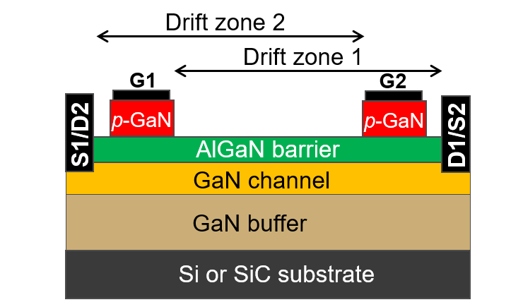
Schematic of a bidirectional GaN transistor with two gates
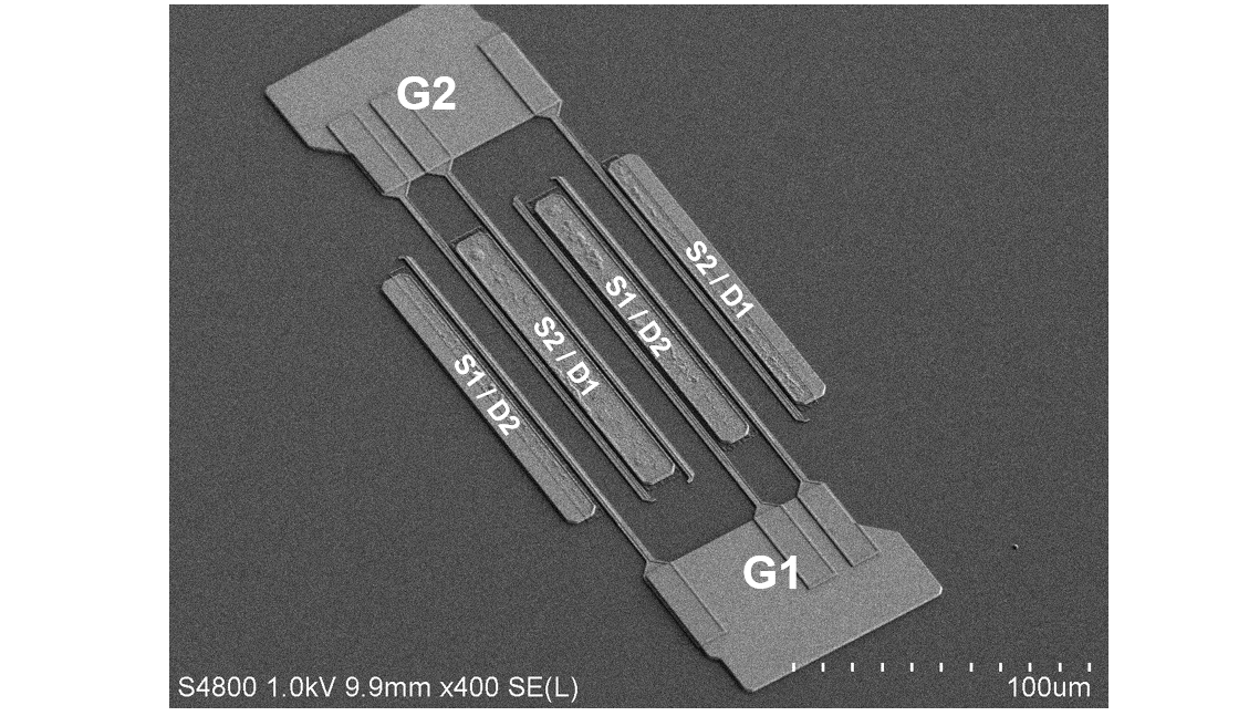
Scanning electron micrograph of a bidirectional transistor structure with source, gate and drain metallizations
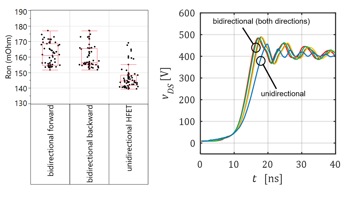
On-resistance (left) and 10 A off-transient (right) of a bidirectional GaN transistor in both operating directions, comparison to an equally sized unidirectional GaN transistor
Very efficient conver topologies without intermediate DC link can be used for AC power converters like T-type or matrix converters. However, bidirectional transistors are needed as switches that have to conduct or to block current in both directions. In silicon technology, only vertical devices can be used for voltages above 200 V, which makes a bidirectional switch very complex.
Bidirectional functionality for high voltages is possible straight forwad when using the unipolar lateral 600 V GaN transistor technology. Here, two gates are inserted into the drift region and the transistor channel in-between these gates can be used for both directions of device operation. As a consequence, the on-state resistance of the bidirectional transistor is only slightly increased with respect to the standard unipolar version.
At FBH, we simulataneously process unipolar and bipolar transistor structures on the same wafer. Breakdown voltages are identical and on-state resistance of the bidirectional device version is only 10% as compared to the unidirectional version. The switching characteristics are identical for both operation directions of the bidirectional GaN transistor.
