Wafer Processes & Masks
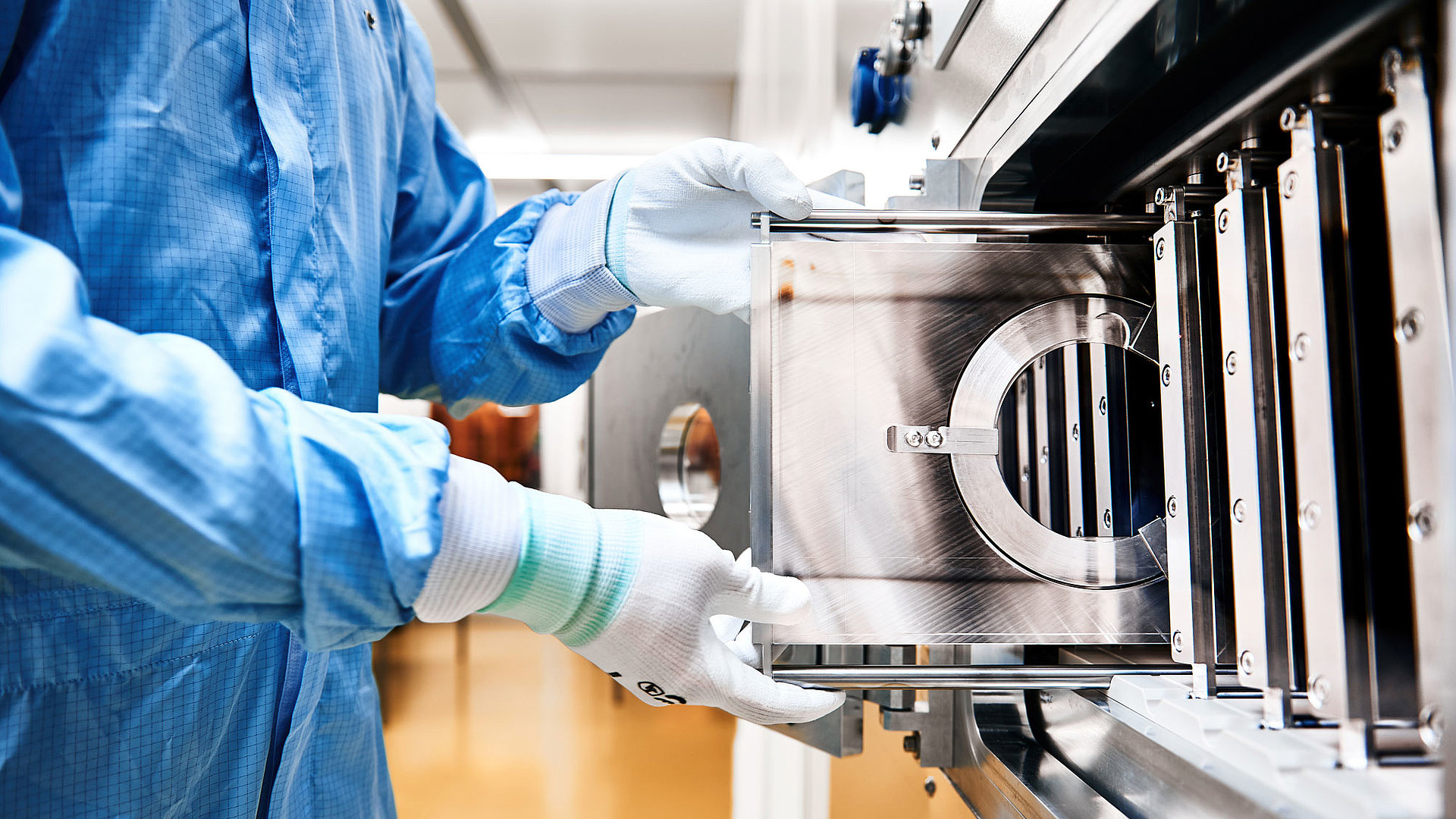
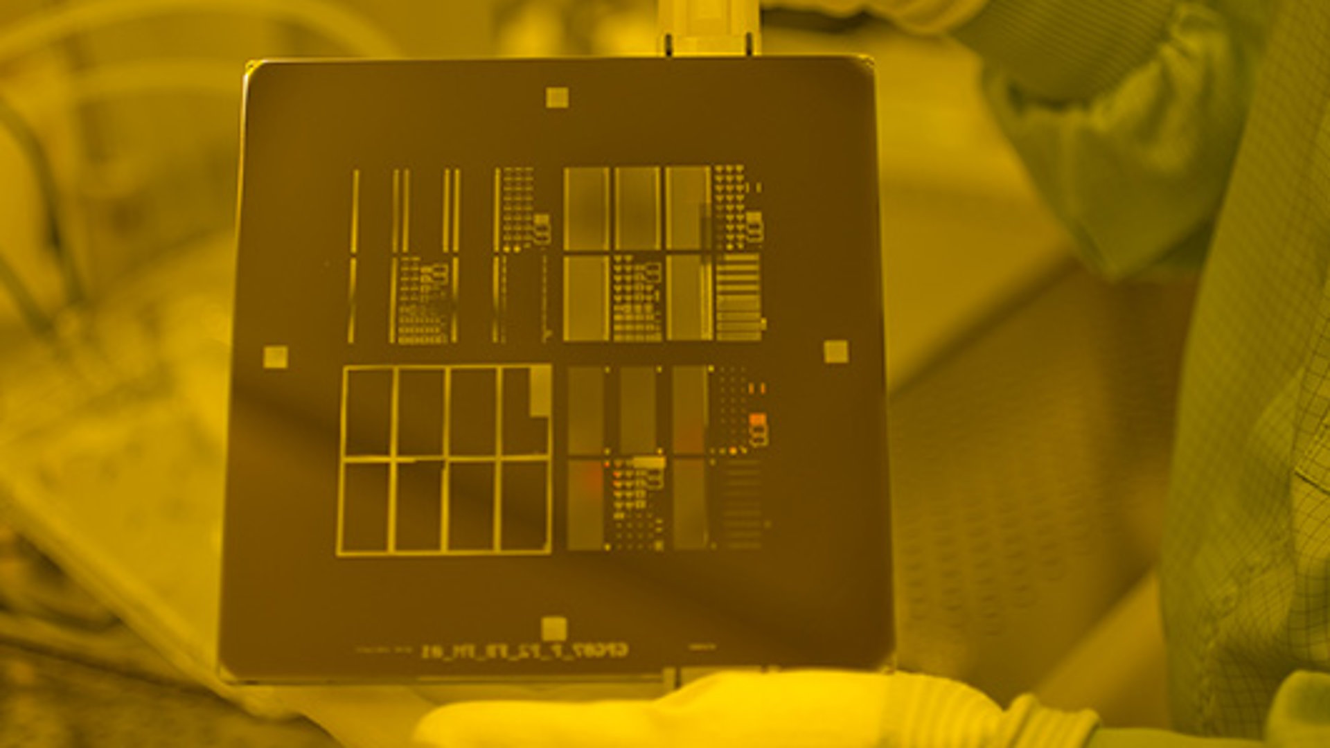
We have been successfully offering our customers individual process steps or process modules according to specific requirements for many years. For this purpose, we use our flexible and industry-compatible process line for III/V compound semiconductors – contact us!
Wafer processes
- technology development for components according to customer specifications
- pilot production of components
- development and implementation of process steps
- lithography up to sub-µm
- etching
- thin film deposition of insulators and metals
- ion implantation
- laser microstructuring
- thinning
- sawing
- in-line analysis during the process
More information about our process technology
Masks & reticles
- chrome-coated masks made of quartz glass
- standard masks 4", 5" and 6"
![[Translate to English:] Technologieangebot des FBH](/fileadmin/_processed_/7/2/csm_Technologieangebot_FBH_2024_1432587108.png "Technology offer: Overview")