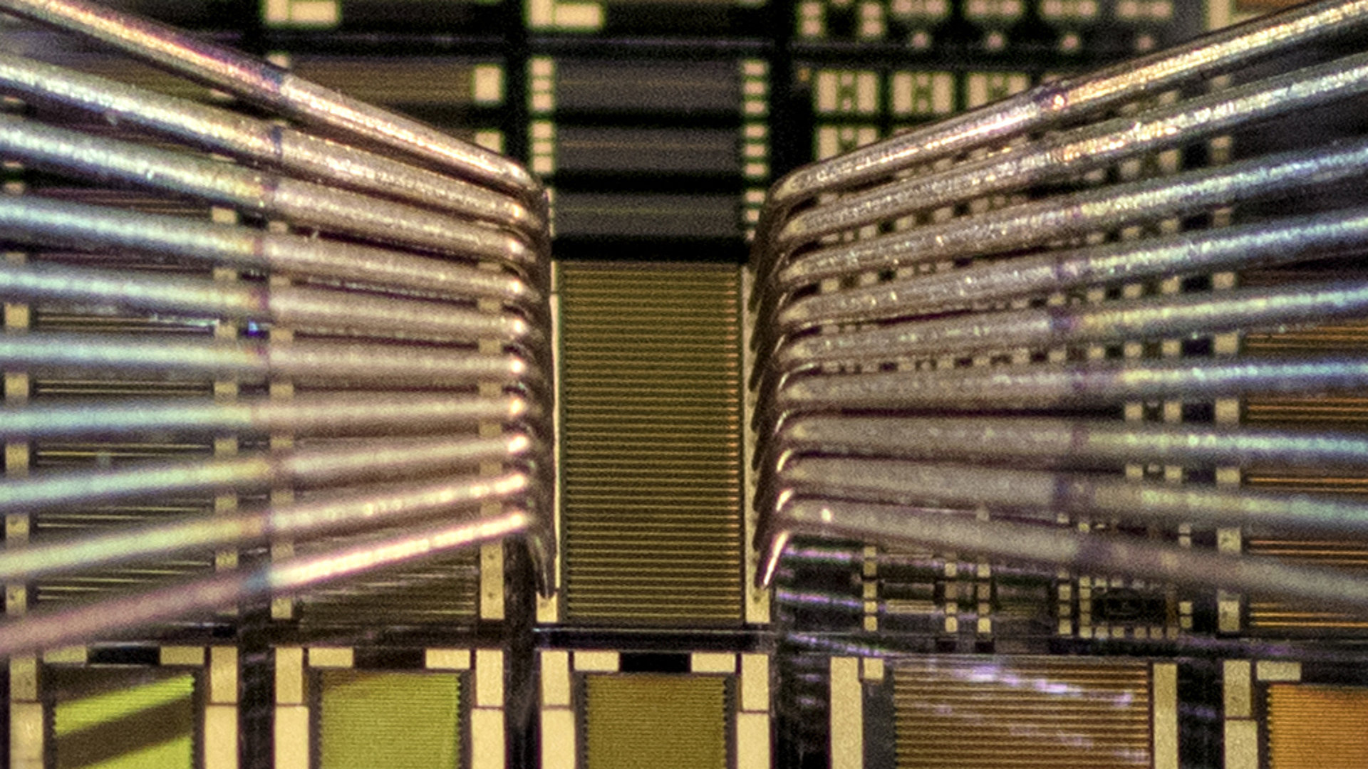
Lateral AlN Transistors
GaN-based switching transistor for power-electronic applications have not yet reached their material limits with respect to on-state resistance for a given blocking voltage. One major reason are dispersion effects that occur with high voltage switching. These are triggered by the compensation doping of the GaN buffer layer that is needed for sufficient breakdown strength. That's why we replace the doped GaN buffer layer with the ultra-wide bandgap material aluminum nitride (AlN).
Structure & advantages of the transistor structure
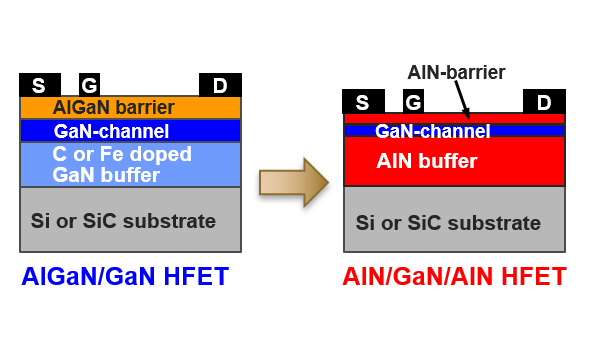
Advancement of an AlGaN/GaN/GaN transistor to an AlN/GaN/AlN transistor
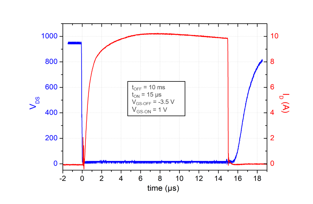
On-wafer measured 950 V/10 A switching transient of an AlN-based 120 mOhm/1200 V transistor
In the new AlN-based transistors, GaN is only needed for the approximately 100 nm thick transistor channel layer. Due to its very high bandgap, AlN enables an extremely voltage-resistant buffer layer. Compensation doping of the buffer can therefore be omitted. The new AlN-based transistors exhibit higher dielectric strength than their GaN-based predecessors with a lower increase in dynamic on-resistance.
We have processed 120 mOhm 1200 V switching transistors on 4-inch AlN-on-SiC wafers grown at FBH, which can be used for switching converters up to the 10 kW class, as demonstrated by the 10 A/950 V switching transients.
The very high thermal conductivities of both the new AlN buffer layer and the SiC substrate result in optimal heat dissipation from the power device. The high electrical insulation capability of both materials simplifies the monolithic integration of the power circuit even for high switching voltages.
