Group III-Nitride Epitaxy
We apply metalorganic vapor phase epitaxy (MOVPE) to grow layer structures based on the III-nitrides (Al,Ga,In)N. These structures are used in optoelectronic devices for the wavelength range from 200 nm to 500 nm and in high power transistors. In the focus of our development are blue-violet laser diodes, UV-B and UV-C LEDs, solarblind photodiodes, and transistors which are designed for high currents, high breakdown voltages and high frequencies. To further optimize these devices, we are also developing substrates and templates with low dislocation densities which allow epitaxial growth of AlGaN layers with high aluminum concentration and reduced strain.


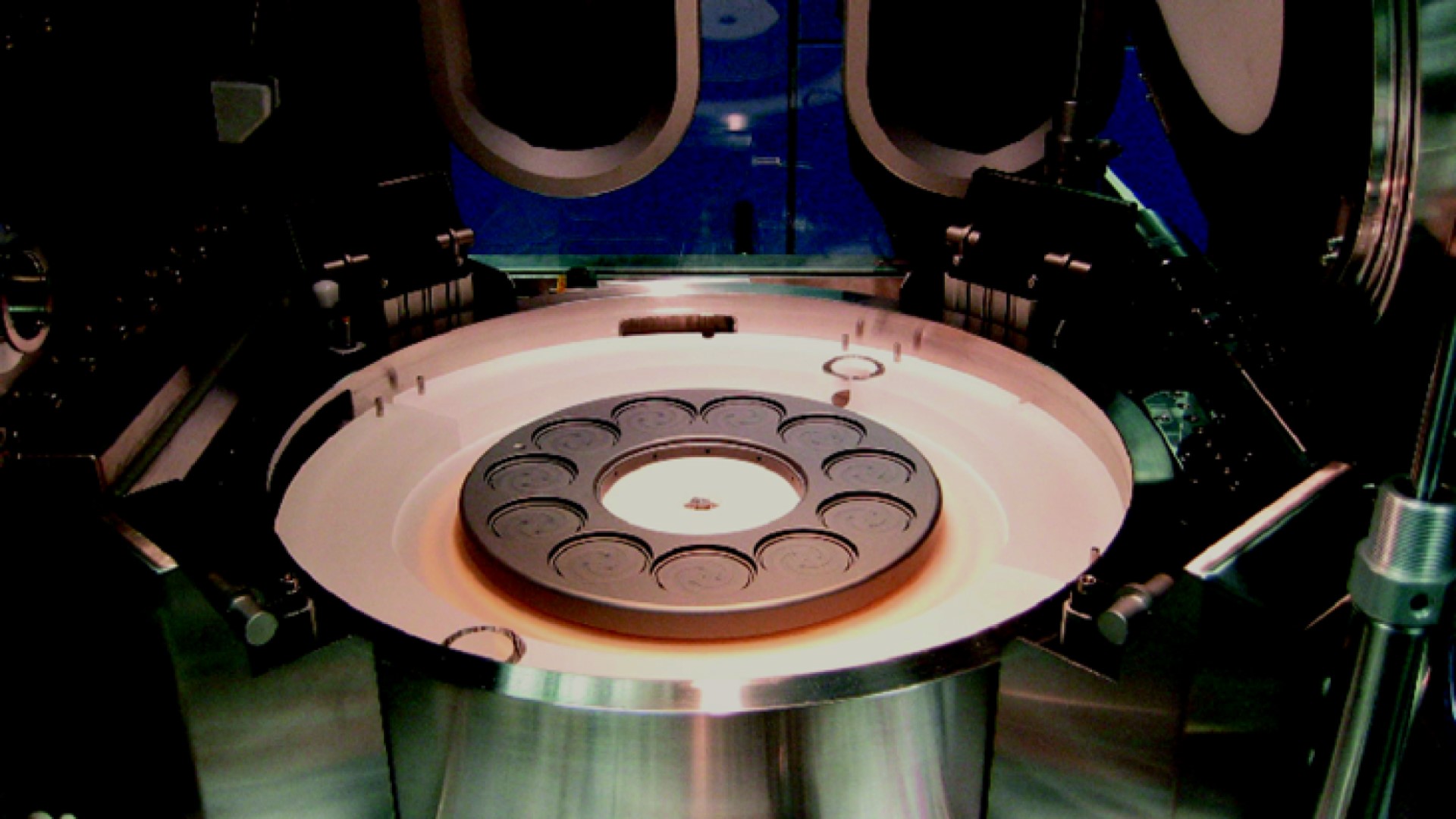
Nitride-based epitaxial growth at FBH is done in five different MOVPE reactors. We use an AIX200/4-RF-S MOVPE system with a capacity of 1×2" to deposit optoelectronic epitaxial structures on GaN substrate, primarily blue-violet laser diodes. An AIX2600G3-HT (11×2") multi-slice system allows growth temperatures of up to 1400 °C to produce high quality AlN layers, for example on sapphire substrate, which are used as templates for UV LEDs. With a high-temperature furnace, the crystal quality can be further improved by heating up to 1700 °C. Another AIX2600G3-HT reactor forms the basis for the GaN HFET activities at FBH on 4" substrate. We use a Close Coupled Showerhead Reactor (6x2") for the fabrication of layer structures for UV LEDs. A second reactor of this type is used for AlN-based heterostructure field effect transistors (HFET) within the funding program of "Research Fab Microelectronics Germany" as well as for vertical MISFET structures. All MOVPE systems are equipped with in-situ sensor technology (curvature sensor EpiCurveTT from LayTec).
For our customers we realize semiconductor layers with defined optical and electrical properties:

