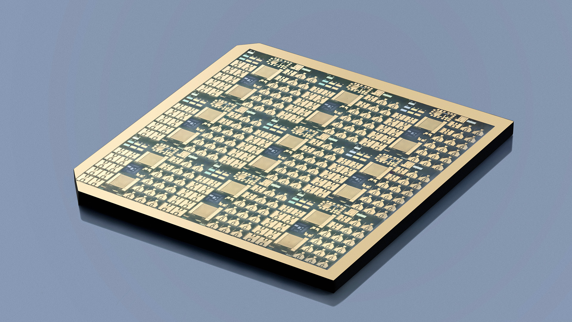
Gallium Oxide Power Transistors
Due to the increasing demands on higher dielectric strengths of electronic components in power electronics, the FBH is intensively focusing on new semiconductor materials which have a high potential to meet these requirements. The promising semiconductor gallium oxide (β-Ga2O3) is characterized by a very wide bandgap of around 4.8 eV, from which a high dielectric strength with values far above that of gallium nitride or silicon carbide can be derived. This opens up the possibility of a significant reduction in the gate/drain separation in the transistor, so that semiconductor switches can be manufactured even more compactly and efficiently.
Therefore, FBH has research activities in cooperation with the Leibniz Institute for Crystal Growth in recent years regarding the development and processing of lateral and vertical power switching transistors based on β-Ga2O3.
Lateral devices
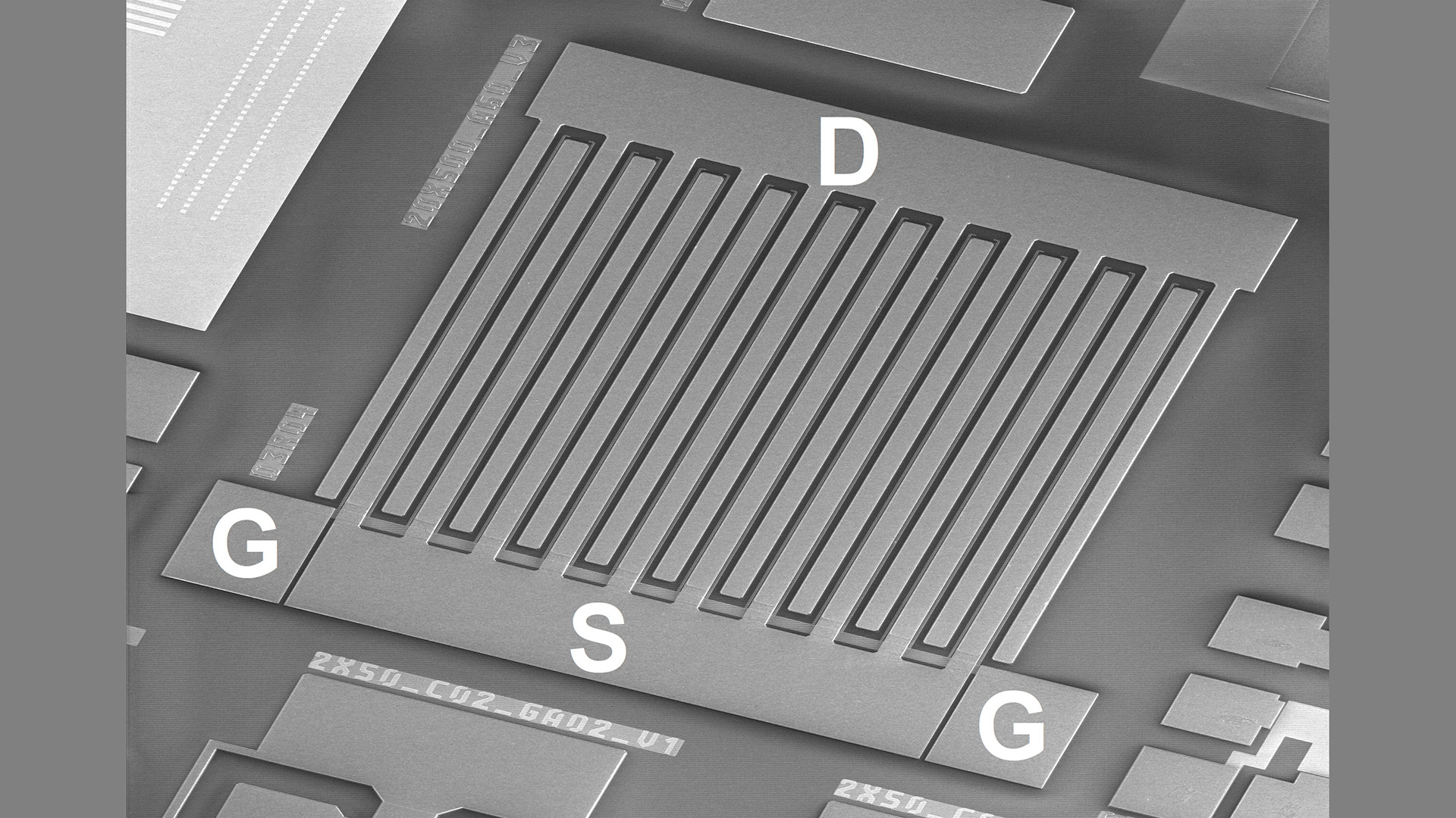
Multi-finger β-Ga2O3 switching transistor with 10 mm total gate width
By optimizing the layer growth and the device processing with regard to the gate topology, it has been possible in previous investigations to produce transistors that are characterized by a high breakdown strength of up to 2.5 MV/cm. In addition, breakdown voltages of 1.8 kV were achieved, resulting in a high power density of 155 MW/cm².
In cooperation with Technische Universität Berlin, the dynamic properties during operation at a drain voltage of 300 V and a drain current of 300 mA were further investigated. Fast and reproducible switching processes with switching speeds of 65 V/ns were measured, which verifies an essential prerequisite for producing even more efficient power switching transistors on the basis of β-Ga2O3 in the future.
Vertical devices
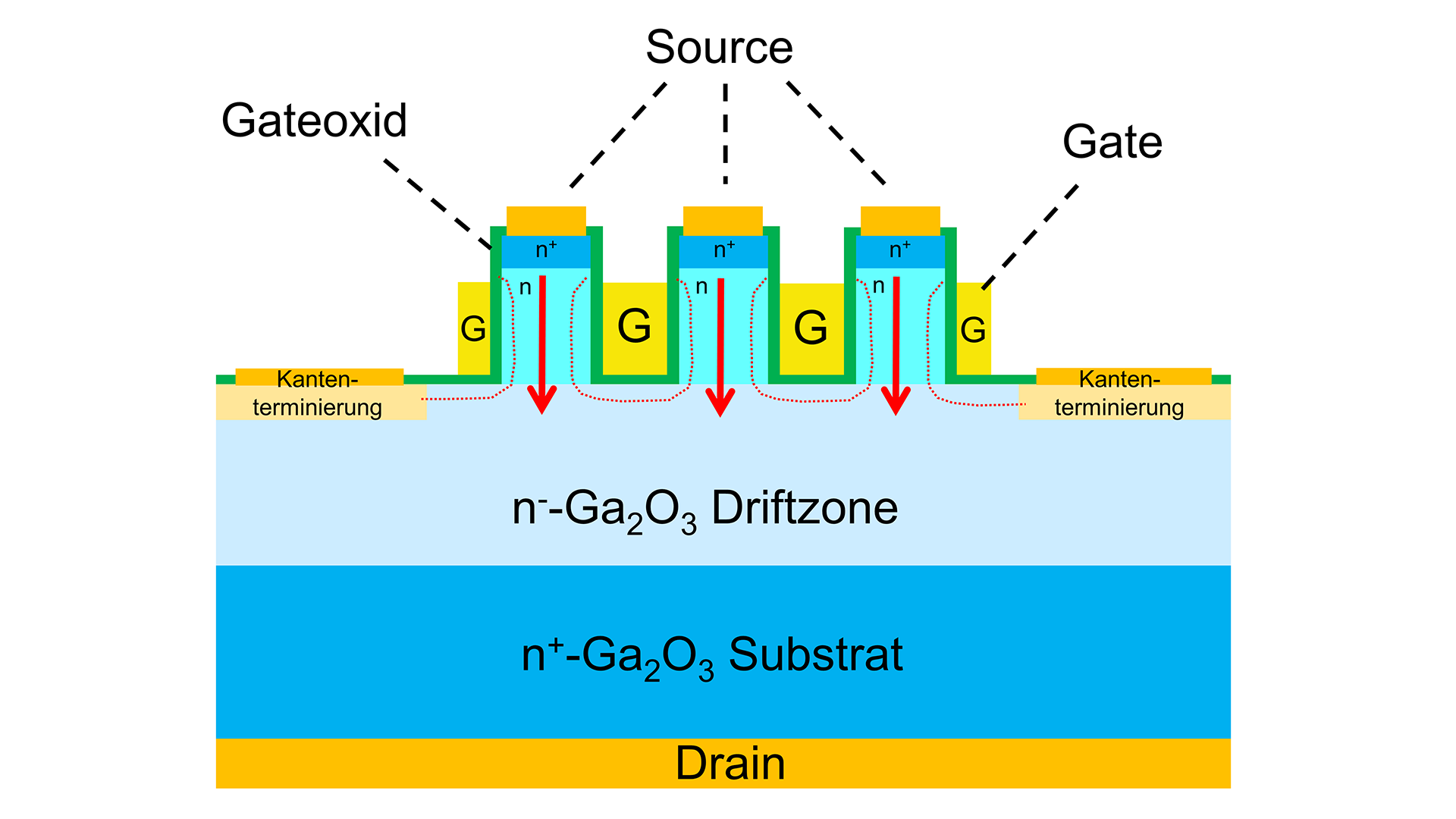
Schematic cross section of the vertical FinFET structures based on the ultra-wide bandgap semiconductor β-Ga2O3 developed at FBH
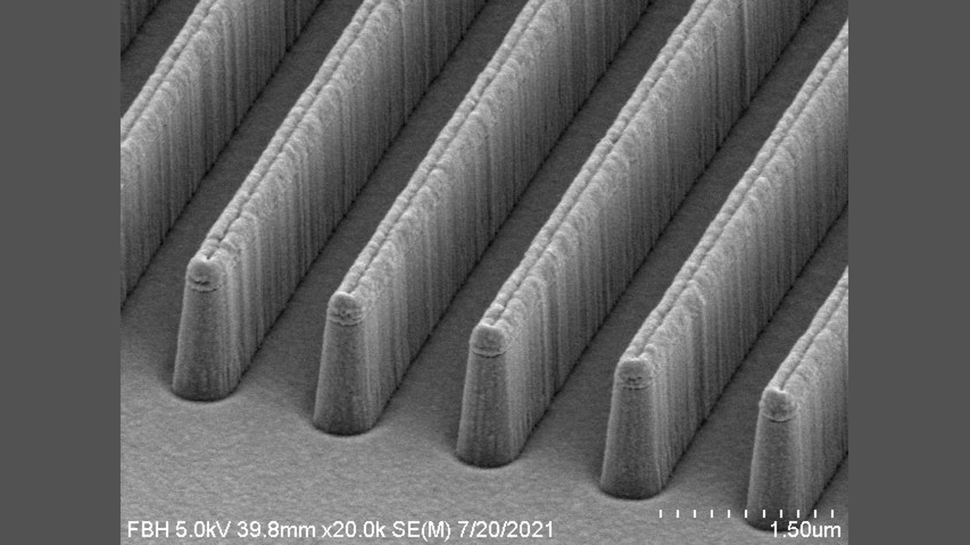
Dry-etched fin structures in β-Ga2O3 featuring a width of 200 nm and a height of 1 µm at a pitch of 1.2 µm with nearly vertical sidewalls
Devices in a vertical structure offer great advantages to better exploit the potential of β-Ga2O3 with its high breakdown field strength. Due to the ideal separation of the high potentials on the top and bottom of the wafer through the epitaxially grown drift zone, the device is significantly less sensitive to surface effects, so that voltages in the range above 1 kV can be switched reliably. In addition, the chip area can be used more efficiently, which results in a significant potential for device scaling.
However, in contrast to lateral device structures, other requirements are placed on material and process technology. For example, conductive substrates are required on which layers of several micrometers thickness have to be grown epitaxially in order to realize a low-doped drift zone.
In cooperation with the Leibniz Institute for Crystal Growth, the FBH is working intensively on the realization of vertical FinFETs based on the semiconductor material β-Ga2O3 within the GoNext project funded by the BMBF and the Leibniz ScienceCampus GraFOx. The effective control of such device is largely determined by the width of the respective fin structures, which means that using electron beam lithography to generate structures in the sub-micrometer range is absolutely necessary. By means of dry chemical etching processes, fin structures that exhibit a high steepness with a width of 200 nm and a height of 1 µm can be produced. This is an essential prerequisite for realizing vertical FinFETs. The project aims at realizing a normally-off vertical Ga2O3 FinFET with a breakdown voltage of 2 kV and an on-resistance of a maximum of 10 mΩ/cm2.
