Mounting of Laser Diodes
Laser chips - based on InAlGaAsP quantum wells on GaAs-substrates as well as InGaN quantum wells on GaN substrates - grown and processed at the FBH require a well-tuned mounting technique. The assembly of the chips has to ensure small thermal resistivity as well as minimal mechanical stress, e.g., by matching the thermal expansion coefficient of chip and heatsink. The light-emitting facets of edge-emitting diode lasers have to be positioned exactly to avoid shadowing the emitted beam. It is crucial at the same time to sustain a high heat removal at the facets (due to high facet loads of up to 20 MW/cm² in GaAs-based lasers) as defects are forming at these high loads.

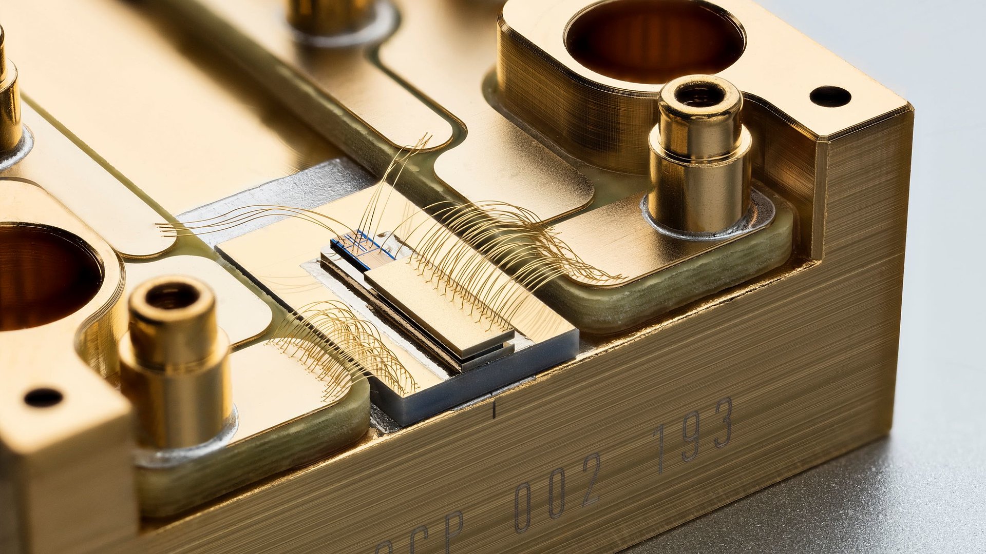
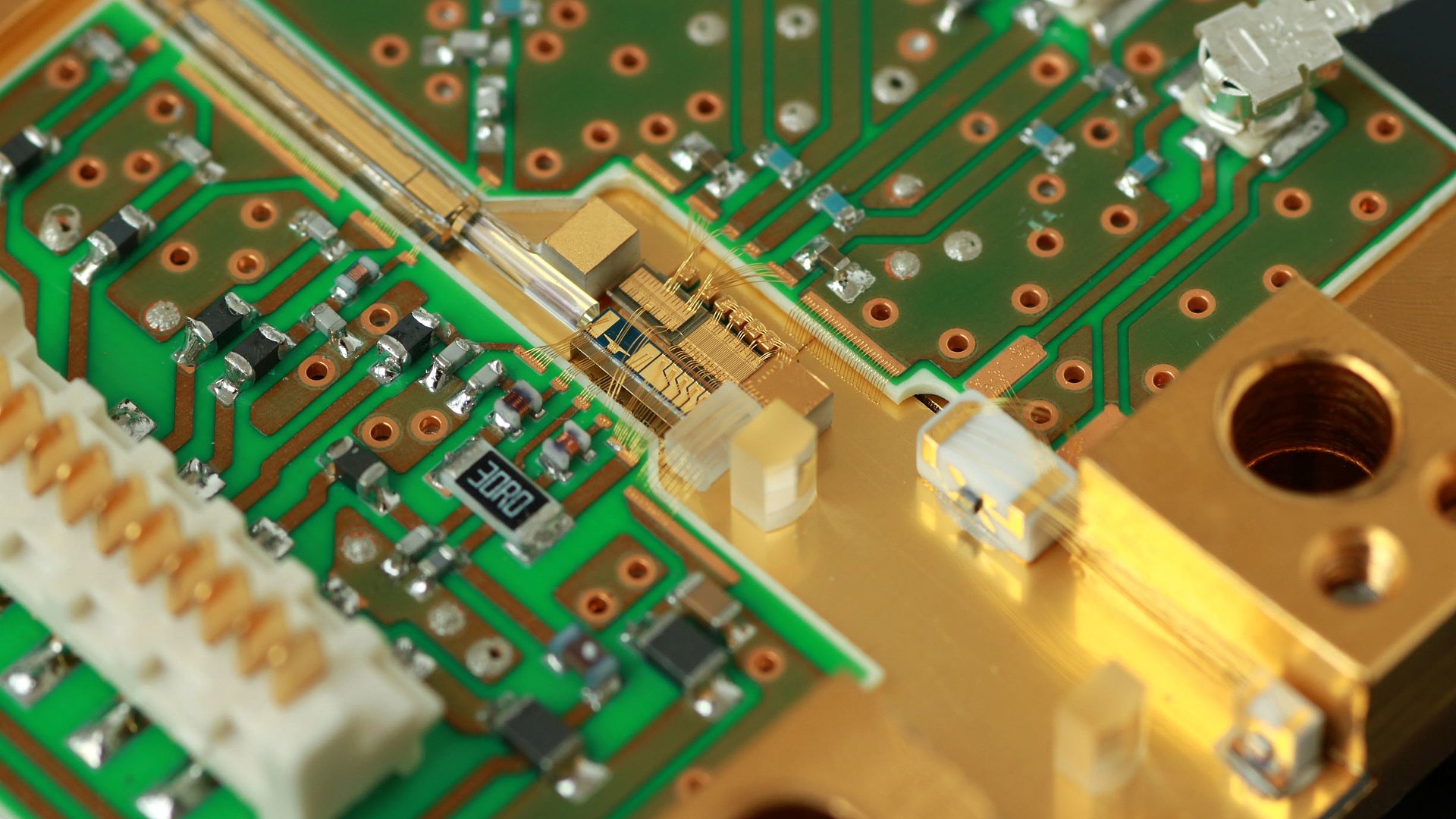
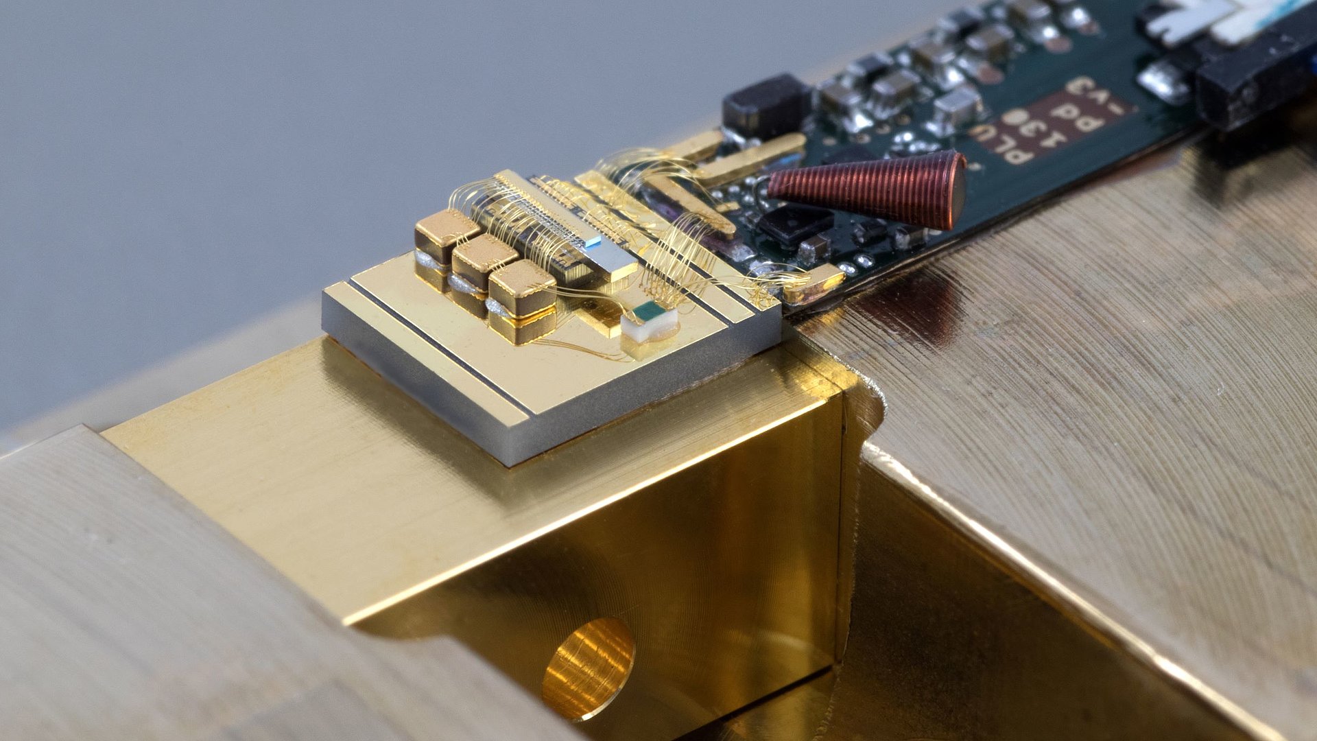

At the FBH, diode lasers are either mounted as single emitters or as laser bars onto submounts made from expansion-matched composite materials such as Cu/W or Cu/Dia or onto AlN, Si, or diamond. More advanced integration of the chips into micro modules (which are, for example, featuring a seed laser, an optical power amplifier, integrated circuits, components for beam shaping etc.) are also being accomplished in the AVT up to the point where turning on of the active parts becomes necessary. Positioning of the 'actively' placed component for optical coupling is completed directly in the laboratories of the individual Photonics Labs.
Techniques
- Die bonding of semiconductor chip, laser bars, modulators
- Fluxless soldering in hydrogen atmosphere
- TS Au wire and ribbon bonding
- Precision placement of laser diode chips onto micro-optical benches
- Laser diodes mounted together with GaN driver circuits for optical ps-pulse generation - a combination of laser mounting and microwave mounting techniques
- Stacked arrays for very high powers