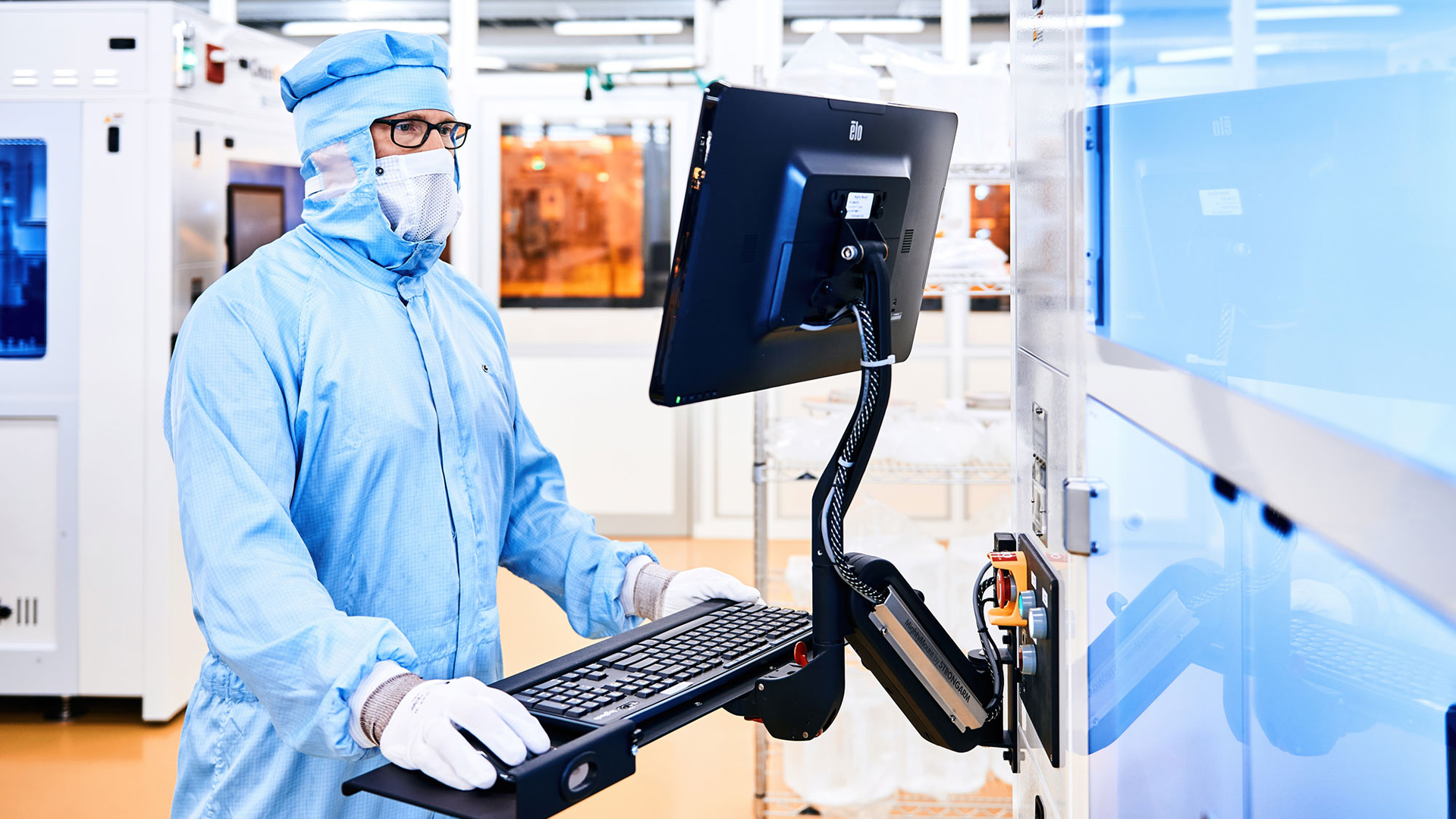
Process Technology Department
We process wafers from 2" to 100 mm and different substrates (GaAs, InP, Si, SiC, sapphire, GaN) with high reproducibility. With modern process equipment equipped to industrial standards, we develop processes quickly, transfer them to small series if required, or transfer process modules to partners.
The process line of our department covers all technologies, from structuring of the epitaxial wafer to chip separation for packaging. More about our processes and technologies.