Transferred substrate InP/GaAsSb heterojunction bipolar transistor technology with fmax ∼ 0.53 THz
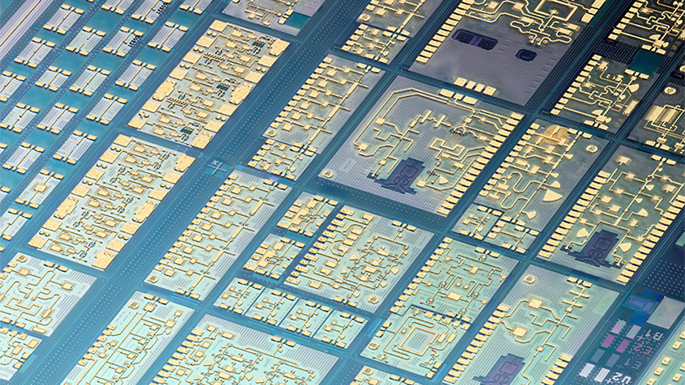
Fig. 1: Photograph showing a wafer part with several MMICs realized in the InP process module heterointegrated on IHP’s SiGe BiCMOS technology.
As InP-based semiconductors exhibit outstanding cut-off frequencies and large breakdown voltages, they provide comparably high output powers in the terahertz frequency range.In recent years, FBH has developed an InP MMIC process, allowing to transfer the epitaxial layers to various kinds of host wafer substrates. This process offers two distinct advantages. First, FBH’s InP MMIC technology can, for example, be hetero-integrated as a module on IHP’s SiGe BiCMOS process technology [1]. Fig. 1 shows a photograph of such a wafer part with serval MMICs. The power generation capability offered by the InP DHBT technology can be combined with the circuit complexity of the SiGe BiCMOS technology on a single microchip, thus avoiding coupling losses and reducing integration costs. Full RF front ends for terahertz applications can be manufactured. Second, the process facilitates to structure the epitaxial layer stack from the emitter and collector side and therefore allows fabricating vertical transistors. Unnecessary InP material is replaced by a polymer with excellent high frequency properties, thus reducing parasitic capacitances as compared to the standard triple mesa process. Therefore, high cut-off frequencies can be achieved even with relatively large transistor dimensions.
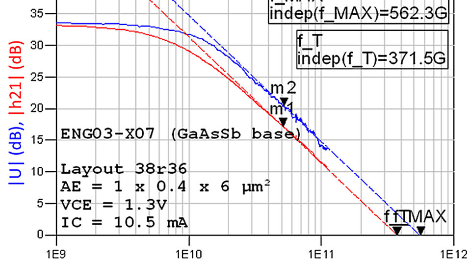
Targeting higher output powers, FBH has applied epitaxial structures with a GaAsSb base grown at ETH Zurich to its unique transfer substrate process for the first time [2]. With a GaAsSb base higher breakdown voltages (here > 4.5 V) can be reached than with a comparable InGaAs base. With an emitter width of 0.4 µm, cut-off frequencies fT = 360 GHz and fmax = 530 GHz are achieved. Further scaling of the transistors is ongoing and will lead to outstanding transistor and circuit performance.
This work was supported in part by the Leibniz Association within the Leibniz Competition projects THz InP HBT. Further funding was provided from the European Commission’s Horizon 2020 program within the Ultrawave project.
Publications
[1] N. Weimann, D. Stoppel, M.I. Schukfeh, M. Hossain, T. Al‐Sawaf, B. Janke, R. Doerner, S. Sinha, F.‐J. Schmückle, O. Krüger, V. Krozer, W. Heinrich, M. Lisker, A. Krüger, A. Datsuk, C. Meliani, B. Tillack, "SciFab–a wafer‐level heterointegrated InP DHBT/SiGe BiCMOS foundry process for mm‐wave applications", physica status solidi (a) 213.4 (2016): 909-916.
[2] N. Weimann, T. Johansen, D. Stoppel, M. Matalla, M. Brahem, K. Nosaeva, S. Boppel, N. Volkmer, I. Ostermay, V. Krozer, O. Ostinelli, C. Bolognesi, "Transferred substrate InP/GaAsSb heterojunction bipolar transistor technology with fmax > 0.53 THz", IEEE Transactions on Electron Devices, DOI: 10.1109/TED.2018.2854546 (2018).

