InP high-speed transistors and integrated circuits in transferred substrate technology
Research on high-speed transistors is driven by applications for imaging and wide band communications. Recent technical advances of InP-based transistors with several hundred gigahertz (GHz) operating frequencies together with their outstanding material properties qualify them as key components in such systems.
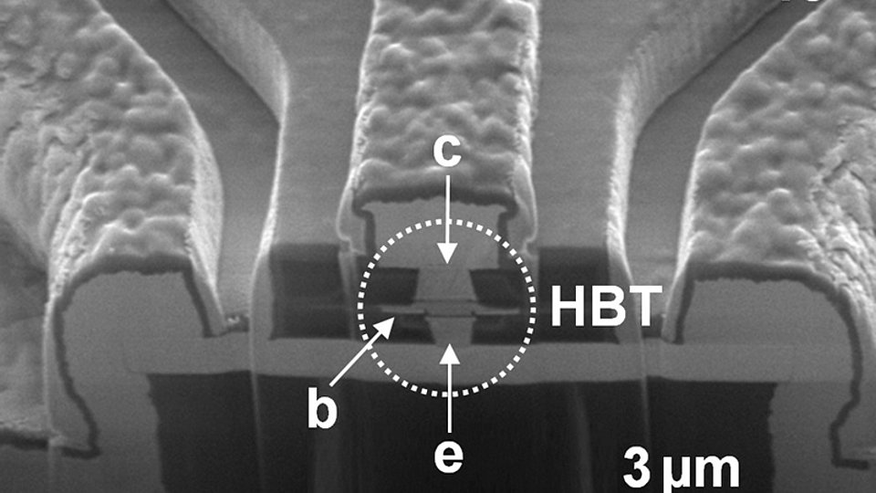
At FBH, a transferred substrate (TS) technology has been established to optimize high frequency and power performance of InP heterojunction bipolar transistors (HBT). The 3" wafer-level process enables lithographic access to both the front- and backside of the HBT aligned to each other. The resulting linear device set-up in Fig. 1 eliminates dominant transistor parasitics and relaxes design trade-offs. The essential step for gaining access to both sides of the epitaxial structure is to completely remove the supporting substrate. Therefore, a robust adhesive wafer bonding procedure via benzocyclobutene (BCB) has been developed. It yields a homogenous, crack- and void-free composite matrix of transistors transferred on a wafer-level scale.
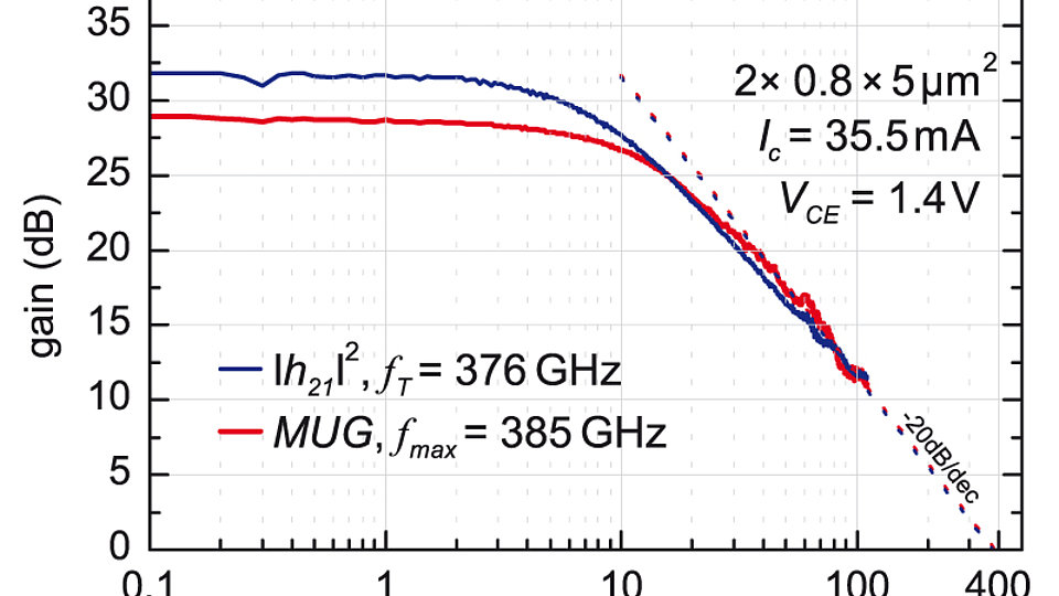
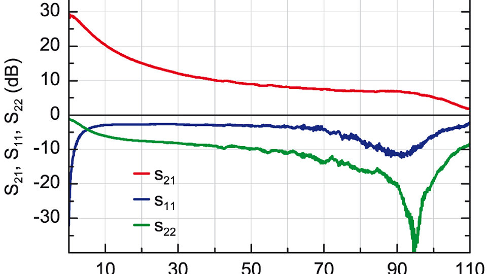
The optimized device topology manifests in excellent HBT performance. Transistors with 2× 0.8×5 μm2 emitter area, as depicted in Fig. 2, feature fT = 376 GHz and fmax = 385 GHz at breakdown voltages BVCEO > 4.5 V. They combine high frequency performance with saturated output power Pout > 14.2 dBm @77 GHz and an inherently good matching to 50 Ω. The highly scalable device architecture is capable to even further increase high frequency as well as power performance in the future. Power amplifiers have been designed and realized in TS technology for 90 GHz operation. Their S-parameter measurements shown in Fig. 3 confirm a good agreement with modeling.
Currently, the innovative transistor set-up is utilized in an ongoing project to integrate InP-based circuits ontop of BiCMOS wafers heterogeneously.
Publication
T. Al-Sawaf, C. Meliani, W. Heinrich, and T. Krämer, "<link /fileadmin/fbh-berlin/english/ver12/pub16.htm _blank internal-url-new-window>W-Band Amplifier with 8 dB Gain Based on InP- HBT Transferred-Substrate Technology", Proc. German Microwave Conference, Ilmenau, Germany, 12–14 March 2012.
FBH research: 30.03.2012


