GaN HFETs with high current and high breakdown voltage using Si-doped AlGaN back barrier
For power conversion for example in e-cars or photovoltaic systems, transistors with low on-state resistance and high voltage stability are required. GaN HFETs here have a high potential. In order to increase the breakdown voltage, Fe- or C-doped GaN buffers can be used. However, due to the higher barrier in comparison to an undoped buffer the carrier concentration in the channel is reduced. The same holds true for AlGaN buffers, which additionally increase the thermal resistance.
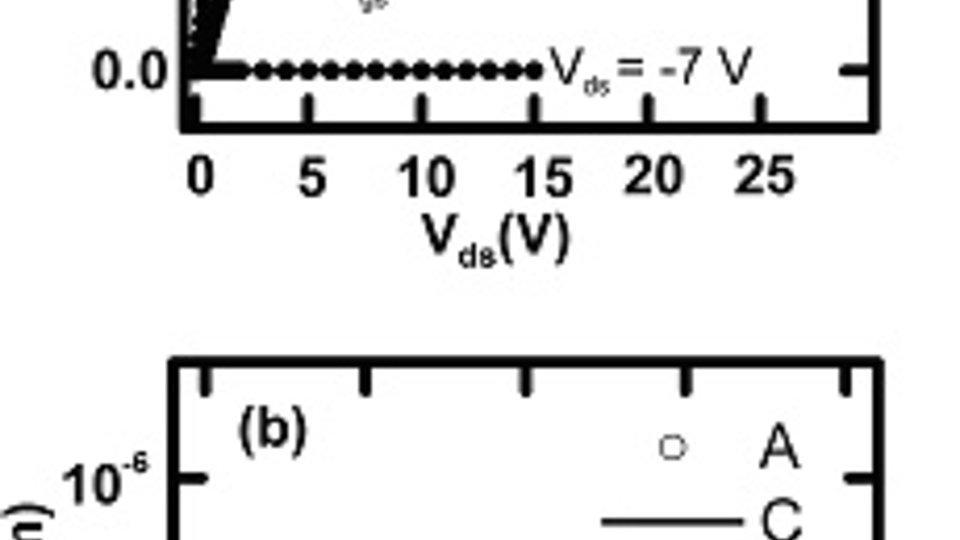
The reduction in the carrier concentration in the channel can be compensated by n-type doping of a thin (10 nm) AlGaN back barrier between the C-doped buffer and the channel layer. The electrons supplied from this layer result in a nearly doubled current Ids,max in comparison to an otherwise identical transistor structure without this AlGaN carrier supply layer (Fig.1 top), A: only C-doped GaN buffer; C: with Si-doped AlGaN back-barrier). Consequently the on-state resistance is improved too. At the same time the voltage stability is not compromised or even slightly improved as can be seen from the current under pinch-off conditions (Fig. 1 bottom). Leakage currents are low up to the measurement limit of 1000 V.
A thin n-doped AlGaN layer between the highly resistive C-doped GaN buffer and the undoped channel thus can significantly improve the trade-off between on-state resistance and breakdown voltage of GaN HFETs for power switching applications.
References:
[1] E. Bahat-Treidel, F. Brunner, O. Hilt, E. Cho, J. Würfl, G. Tränkle, "AlGaN/GaN/GaN:C Back-Barrier HFETs With Breakdown Voltage of Over 1 kV and Low RON × A", Trans. Elect. Dev. IEEE, vol. 57, no. 11, pp. 3050-3058 (2010).
[2] E. Cho, F. Brunner, R. Zhytnytska, P. Kotara, J. Würfl, M. Weyers, "Enhancement of channel conductivity in AlGaN/GaN heterostructure field effect transistors by AlGaN:Si back barrier" accepted for publication in Appl. Phys. Lett. (2011).
[3] Patent application DE 10 2011 004 080.3 (2011).
FBH research: 18.08.2011
