Gallium oxide MISFETs for power electronics applications
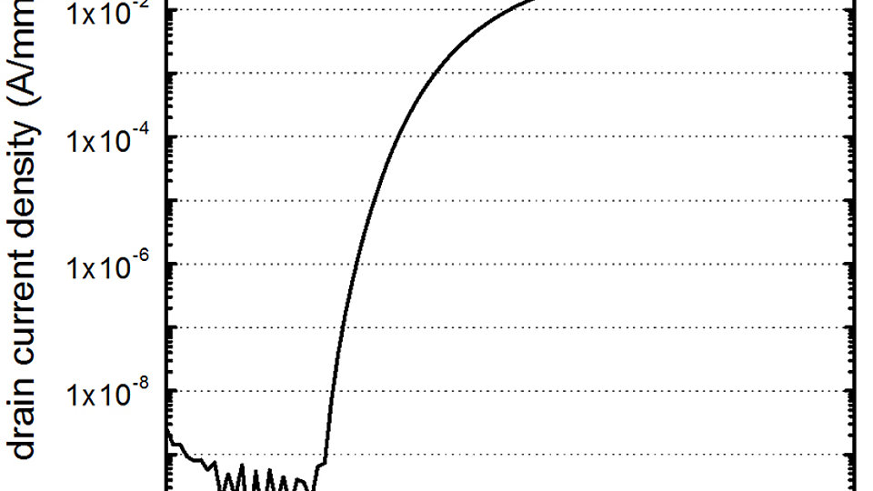
Fig. 2: Transfer characteristic of a β-Ga2O3 (100) MISFET with 40 nm Al2O3 PEALD layer measured at a drain voltage of 10 V
Gallium oxide (β-Ga2O3) is a promising ultra-wide-bandgap semiconductor for future power electronics applications due to its outstanding material properties like breakdown field strength even higher than for GaN. State-of-the-art metal-isolator-semiconductor field-effect transistors (MISFETs) were successfully processed at FBH on β-Ga2O3 epitaxial material from the Leibniz Institute for Crystal Growth (IKZ). The gallium oxide substrates were also fabricated at IKZ using Czochralski bulk crystal growth method.
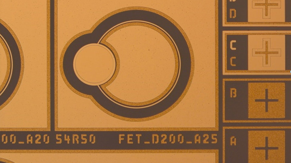
At FBH, a suitable processing scheme based on circular transistor layouts has been developed [1]. This allows processing and operating transistors without the need for device isolation. Fig. 1 shows such a circular β-Ga2O3 MISFET with the source electrode in the center of the structure. Gates with a gate length of 3.5 µm were formed by Pt/Au metal electron-beam evaporation and subsequent resist lift-off. For the β-Ga2O3 MISFETs a 40 nm Al2O3 layer was deposited by plasma-enhanced atomic layer deposition (PEALD) combined with in-situ NH3 plasma surface pre-treatment prior to gate metallization. This process step has been performed in cooperation with SENTECH.
Source and drain ohmic contacts were fabricated by Ti/Au metallization after surface conditioning in BCl3-Ar plasma followed by a rapid thermal annealing step. Linear I-V characteristics and low contact resistances down to 3 Wmm were obtained. All pad areas for the three terminals were reinforced by 750 nm thick Ti/Au metallization in order to withstand direct probing on the inner transistor area. Finally, the devices were annealed at 350°C using an optimized procedure. This treatment has turned out to be crucial for achieving low leakage currents.
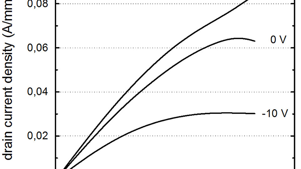
Fig. 2 shows the transfer characteristic of a β-Ga2O3 (100) MISFET measured at a drain voltage of 10 V. The transistor pinches off at around -23 V. Subthreshold drain and gate currents are below 10-10 A/mm. The measurement was limited by current resolution of the standard set-up used. This result gives a large ION/OFF ratio of higher than 109. An output characteristic of the β-Ga2O3 (100) MISFET is presented in Fig. 3. At drain voltage of 25 V drain current levels of 84 mA/mm could be demonstrated at +10 V gate bias. These are state-of-the-art results [2].
In conclusion, by combining high-performance β-Ga2O3 epitaxy with optimized processing and high-quality Al2O3 PEALD gate insulator technology state-of-the-art devices could be realized. The results demonstrate a promising technology baseline towards larger β-Ga2O3 devices for power electronics applications.
Publications
[1] Kurpas, P., “β-Ga2O3 (100) MISFETs for power electronics applications”, paper to be presented at 41th WOCSDICE - Workshop on Compound Semiconductor Devices and Integrated Circuits 2017.
[2] Higashiwaki M., “Current status of Ga2O3 power devices”, Jpn. J. Appl. Phys. 55 1202A1 (2016).


