Flip-chip mounted UV-B LEDs with optical powers in the milliwatt range
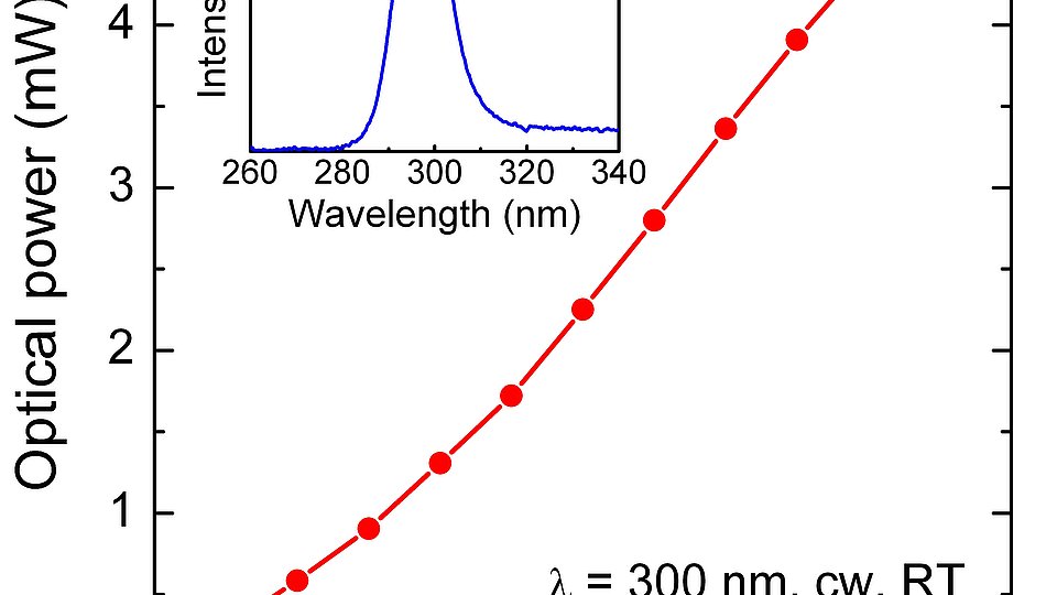
Fig. 1: Optical power-current characteristics of a mounted UV-B LED with an output power of ≥5 mW and emission spectrum at a current of 20 mA.
The application fields of ultraviolet (UV) emitters in the 300 nm to 320 nm wavelength range are manifold: ranging from material processing such as hardening or surface treatment of plastics, paints and finishes to medical applications like phototherapy of skin diseases. One of the benefits of UV light generated by light emitting diodes (LEDs) is that the wavelength can be optimally tailored to fit the application. Furthermore, LED light sources can be realized with compact form factors and, unlike mercury lamps, do not contain toxic substances. Within the regional growth core Berlin WideBaSe, FBH develops UV-B LEDs with high optical power and efficiency in close collaboration with TU Berlin (TUB) and local industry partners. After successful optimization of the fabrication technology we managed to increase the optical power of the devices into the milliwatt range, which is comparable or even better than international record values for this wavelength range.
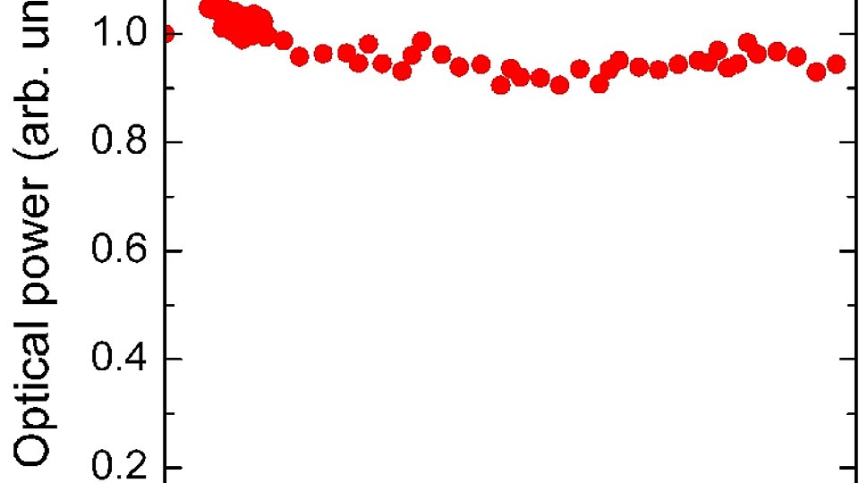
The design and the epitaxial growth conditions of the semiconductor layer structure were found to be the key to improve the LED efficiency. Using AlN buffer layers deposited on sapphire substrates at temperatures ≥1400 °C together with thick Si-doped AlGaN layers, templates for light emitting layers were fabricated whose dislocation density is in the range <1010 cm-2. Moreover, the composition and the doping of the electron blocking layer, which is intended to prevent electrons from overflowing to the p-side of the diode, were carefully optimized. Selected wafers of this first generation were used to process bottom-emitting LEDs which were flip-chip mounted on AlN submounts using hard-solder and measured on copper heat sinks in a calibrated integrating sphere. Fig. 1 shows that the LEDs feature maximum output powers of up to 5 mW at an emission wavelength of 300 nm. Moreover, degradation studies as presented in Fig. 2 show lifetimes of the LEDs of several hundred hours with very little degradation after the burn-in. Further optimization steps allowed to improve the performance of the LEDs even more. UV-B LEDs of the second generation, which were fabricated after these optimizations, reproducibly feature external quantum efficiencies in the range 0.5 to 1 % in on-wafer measurements. In the near future those LEDs will be available as mounted chips and allow us to build first demonstrators for the applications mentioned above.
FBH research: 14.09.2012

