Efficient Microwave Power Transistors for L- and S-Band Applications
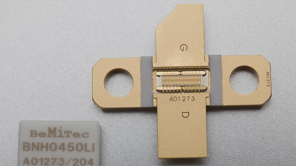
Highly efficient GaN- based microwave power transistors are implemented into modern communication and radar systems to an ever increasing degree. Often complex microwave systems are only possible if compact and highly efficient devices can be integrated within a small volume. In cooperation with its spin-off company Berlin Microwave Technologies (BeMiTec) FBH develops highly efficient power transistors for output power levels of more than 100 W in the frequency range between 1 and 3 GHz. Well adjusted optimizing efforts in materials technology (epitaxy), device processing, general device design including layout as well as chip mounting techniques into a suitable microwave package are key for the development of such devices. Consequently our activities led to promising devices which are combining high power density and high absolute power levels with high efficiency. The devices are mounted into a microwave package according to fig. 1 and are available for implementation into microwave systems.
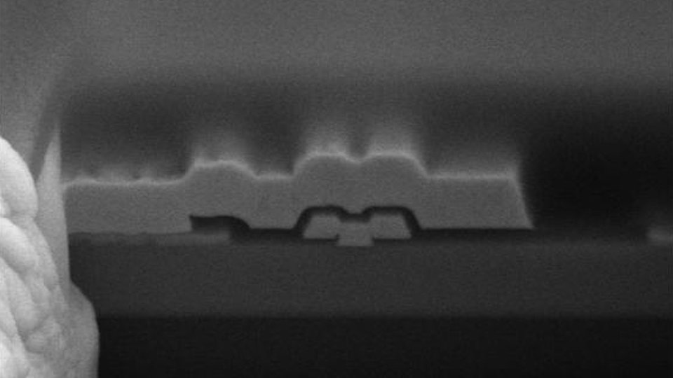
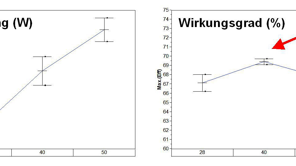
Decisive for the development of transistors showing high output power and efficiency at the same time has been the careful optimization of field plate technology along with the introduction of ballasting resistors between the individual power cells to avoid parasitic oscillations of the packaged power bars. The intention of field plates (see fig. 2) is to influence distribution and maximum intensity of the electric field in internal devices regions such that for all targeted device operation conditions the field maximum always stays below critical field levels. This is a prerequisite for an increase of device operation voltage (for example to 50 V) and for a linear scaling of output power with operation voltage as shown in fig. 3a). The high power added efficiency of close to 70% obtained along with these optimizations qualifies these devices for implementation in microwave amplifier systems operating at 40 V and above. The high operation voltage in turn leads to a higher level of optimum input and output impedance for power matching conditions and therefore enables either very broadband amplifier systems or, by combining multiple power transistors, very powerful microwave amplifiers with power levels above 200 W.
FBH research: 11.04.2012


