Development of optical microresonators and waveguides – the basis for an error-free analyzer for Bell states
Current developments in modern quantum optical technologies are focused on controlling and regulating the interaction of light with individual atoms and cavities. These complex interactions can be used to encrypt information, to build high-precision clocks or to transmit information in a tap-proof manner. Bell states play a key role in this context. They are a concept from quantum information technology and describe states of quantum entangled particle pairs which show strong correlations.
The three-year EU-funded research project "Error-Proof Bell-State Analyzer (ErBeStA)" aims at developing an error-free analyzer for Bell states. Such an analyzer is a key component for optical quantum computers and quantum communication over long distances, e.g., via fiber optic cables. The availability of such a component would be a milestone for all information technologies. To achieve the project goal, an alliance of seven European research institutions in Denmark, Great Britain, Austria and Germany is combining new developments in the fields of quantum optics and nanophotonics. The strong nonlinearities of Rydberg atoms or single quantum emitters coupled to optical microresonators are to be combined with microscopically small optical waveguide devices. By precisely controlling the propagation of light on the scale of the wavelength of the light, these devices shall enable the desired technological breakthrough.
FBH contributes its expertise in the field of process technology to this highly topical research project. Optical microresonators and waveguides are manufactured in a cleanroom using modern lithography and etching processes. By using stepper lithography, structures with smallest dimensions of 400 nm can be produced; for even smaller dimensions electron beam lithography is available, allowing structure dimensions down to 50 nm. The structures generated in a photoresist are then transferred to the optical material using adapted plasma etching processes. In this project, the use of low-damping silicon oxides is being investigated as optical candidate material to keep losses to a minimum. A particular challenge is to release the tiny structures from the wafer so that the guided light is not attenuated by the wafer while retaining a sufficiently strong mechanical connection between the optical components and the wafer. As a result, the components can be used not only in laboratory set-ups, but also in commercial assemblies.
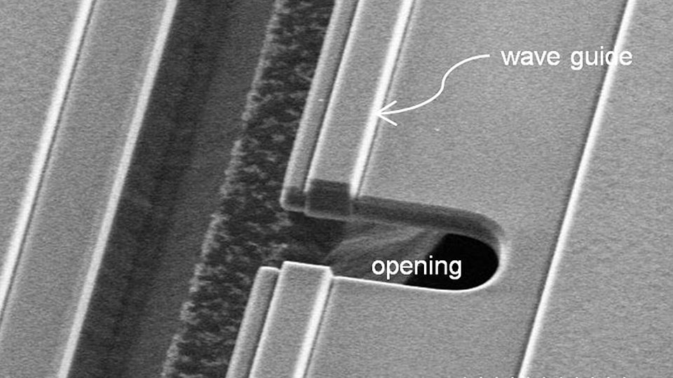
Fig. 1 shows a scanning electron microscope image of a section of such a device fabricated in FBH’s cleanroom. A tiny silicon oxide waveguide of 4 x 4 µm² cross-section is suspended in a thin jib. This design combines sufficient mechanical stability with excellent optical properties. The waveguide has a gap into which atoms can be introduced. This will be done in ultra-high vacuum at very low temperatures by the project partners. They will investigate the interaction of the atoms with laser light guided by the waveguide. From the feedback of these experiments, the design can be optimized and customized components can be produced to build circuits.
