Arrays of ultraviolet micro-LEDs for production, sensing, and communication
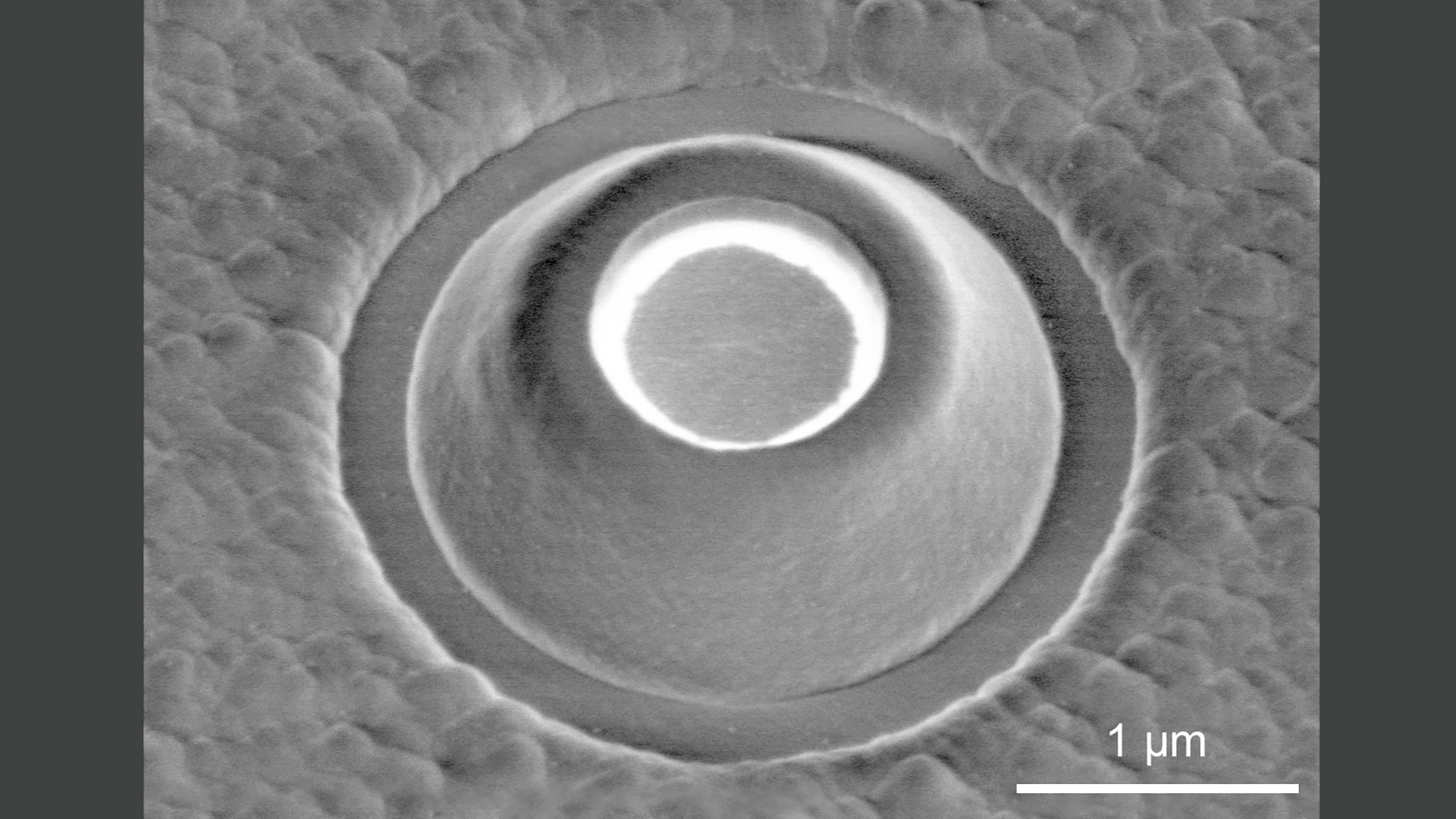
Fig. 1: Electron micrograph of a single UV micro-LED with 1.5 µm diameter.
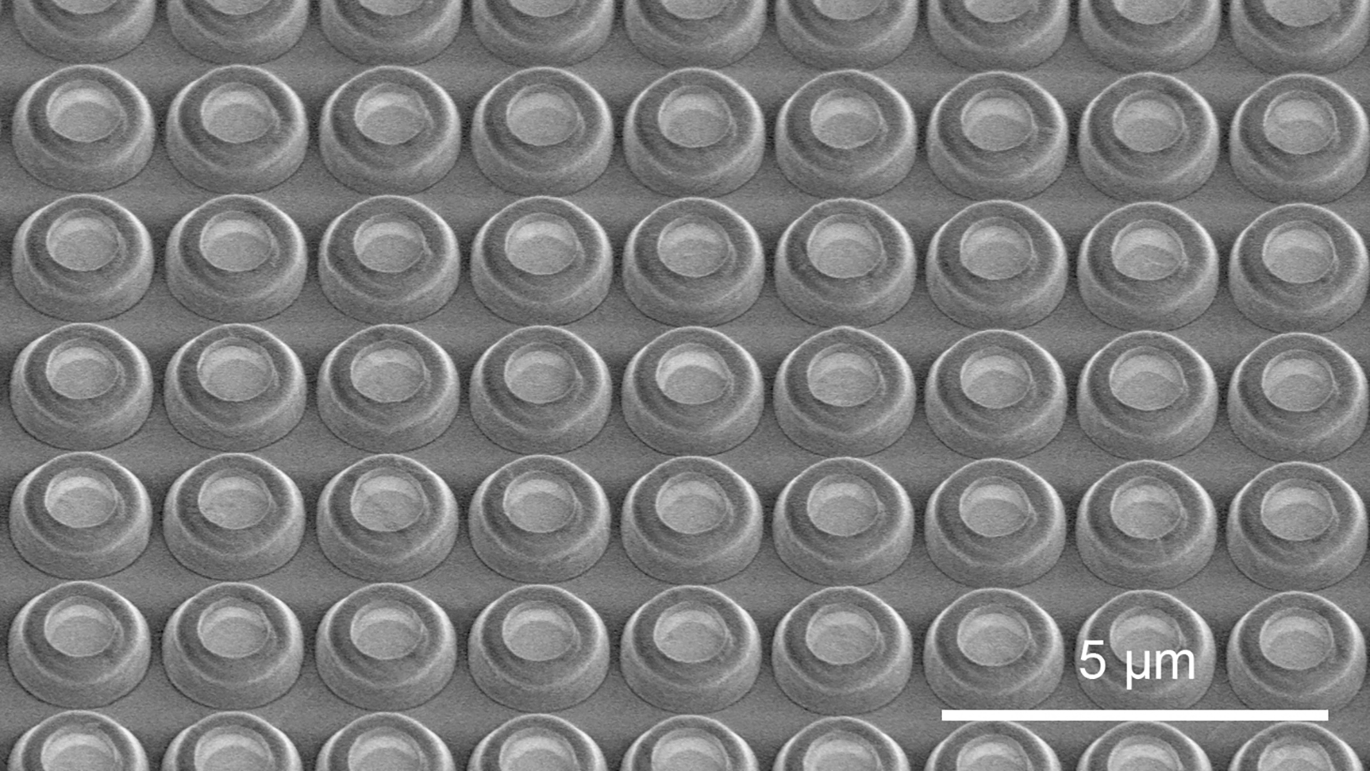
Fig. 2: Electron micrograph of an array of UV micro-LEDs with 2 µm pitch.
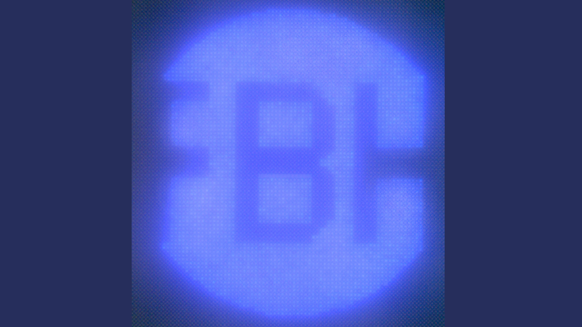
Fig. 3: UV-luminescent pixel array of micro LEDs with a pixel diameter of 1.5 µm and a 2 µm pitch shaped as FBH logo (diameter 158 µm) under the microscope.
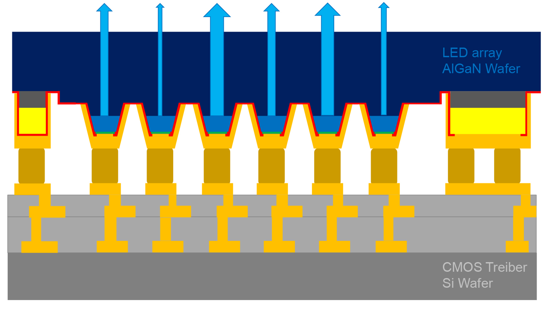
Fig. 4: Concept for a UV micro-LED array bonded on a CMOS back panel.
Red, green, and blue light-emitting diodes (LEDs) with diameters below 100 µm are already widely used, e.g., in display applications. Recently, researchers at the Ferdinand-Braun-Institut (FBH) in Berlin have extended the wavelength range into the ultraviolet (UV) spectrum. This opens up novel applications for these devices, such as in rapid prototyping, mask-free photo lithography, sensing, and non-line-of-sight communication.
At FBH, we have successfully demonstrated the first prototypes of micro-LEDs emitting in the UVB spectral range at around 310 nm. The LEDs feature a small-sized emitting area with diameters down to 1.5 µm. Moreover, they can be closely packed with pitches down to 2 µm to form a two-dimensional array on a chip, resulting in high-resolution UVB emitting areas.
The main challenges in creating such small structures in the AlGaN material system are the high resolution and high alignment accuracy required during the process steps of photo lithography, plasma etching, and material deposition. Since the epitaxially grown wafers usually feature a large convex bow, bow reduction techniques had to be applied.
While currently all micro emitters on a chip are operated simultaneously, the LED pixels in the next step are to be individually addressed via a control chip. This will allow to generate and quickly modulate individual illumination patterns, enabling mask-free photolithography, for example. Individual structures can thus be created on semiconductor wafers easily, quickly, and cost-effectively. The capability of high-resolution UV irradiation patterns opens up new applications. In parallel, FBH scientists are already transferring this technology to UVC LEDs, including far-UVC LEDs with extremely short emission wavelengths around 230 nm. Further work will include the development of integrated mirrors and steps to passivate the etched mesa side walls. This reduces the rate of non-radiate recombination at the perimeter of the micro-LEDs, which gets more dominant with shrinking structure size.