Precise radio-frequency transistor testing with automation and machine learning
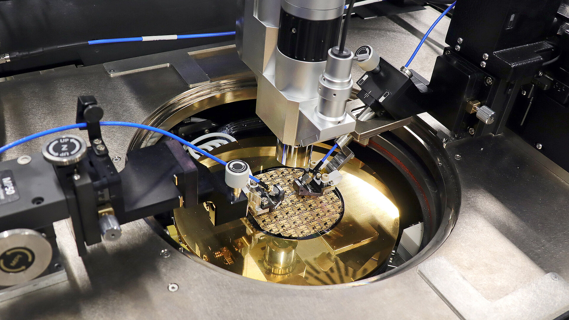
Fig. 1: System used for automatic measurements. The left probe is fixed at the start of the measurements, and the correct position of the device is guaranteed by adjusting the chuck and the right automatic manipulator.
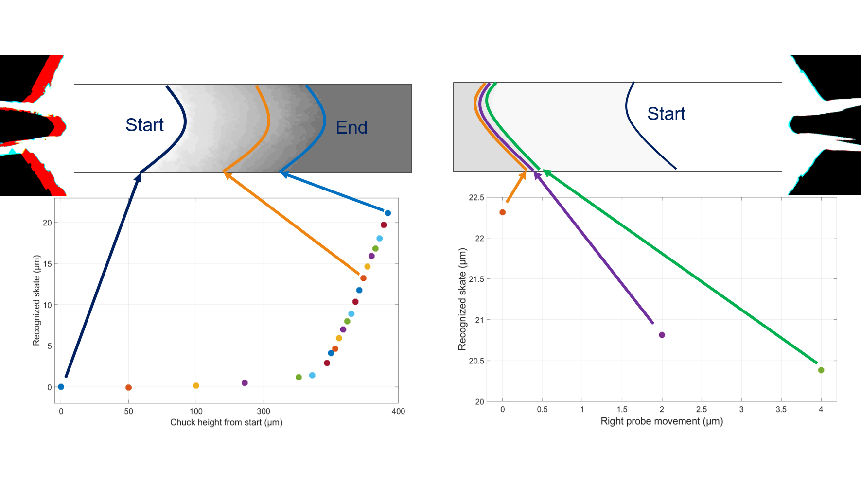
Fig. 2: Adaptive probing as described in [1]. First, the left probe skating (left) is detected continuously until the desired distance is reached. Afterwards, the right probe position is verified (right) and minor adjustments are applied to have the same final position on both sides.
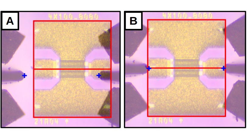
Fig. 3: Box detection and correction as described in [4]. A) A photo of the device is taken and the ML algorithm identifies its boundaries. B) The wafer is adjusted so that the device is placed correctly under the probes.
Radio-frequency (RF) devices, such as power amplifiers or low-noise amplifiers, are used to send and receive signals that enable fast and reliable communication necessary in everyday life. These devices need to be highly efficient and preserve the signal quality as required by modern communication standards. The core of RF amplifiers is the RF transistor, which amplifies the input signals and provides enough power to send them through antennas to the outside world – or, conversely, receives external small signals and amplifies them prior to down-conversion and information extraction.
The ever-increasing demand for more bandwidth and improved efficiency of communication systems drives continuous improvement in the performance of RF circuits and, consequently, the performance of their core element – the RF transistor. For evaluating novel transistor types, precise DC and RF measurements are required. Particularly the on-wafer RF measurements of parameters like maximum power, efficiency, and frequency of operation are very sensitive and prone to errors. In these measurements, high-frequency signals are transferred from the measurement system to the transistor on the wafer through a precisely positioned RF probe.
To improve this measurement procedure, we have developed an enhanced on-wafer probe contacting method capable of probing with an accuracy and repeatability below 2 µm [1,2,3].
The method uses the built-in microscope of the probe station and a programmable manipulator (probe holder) that can automatically move one of the two probes to adjust the probing of transistors across the whole wafer (see Fig. 1). This optically based technique tracks probe-skating – i.e., the probe’s horizontal sliding on the transistor’s pads after contact – in real time and terminates it when the desired skating distance is reached (see Fig. 2). Thereby, irregularities on the wafer, mechanical imperfections of the probing system, and human positioning errors can be compensated, ensuring each device is properly contacted. As a result, this new probing method has been shown to significantly reduce the error contribution from probing in RF measurements up to 50 GHz.
Furthermore, together with TU Berlin, we have developed a machine learning (ML) based algorithm capable of identifying the transistor’s position on the wafer and placing the probes correctly over it with up to 1 µm of accuracy. This ensures that probing is always carried out at the same spot with respect to the probing pads, completely eliminating the need for manual positioning on the device measured. This is achieved with an optical ML-based detection method, which isolates the transistor’s perimeter from the background (see Fig. 3) and thus recognize its position [3]. Furthermore, the method enables recognition of several optical properties of the transistor, including previous probing marks, its type, size, and potential optical damage.
These ML methods, combined with the improved probing technique, enable accurate, fully automatic wafer characterization. This allows for the measurement of many more devices than is normally possible while reducing random and systematic errors and enhancing the overall quality of RF device characterization.
MATADOR (Machine learning for Test Automation and Design-Optimization of RF power transistors) is a collaboration between FBH and Technische Universität Berlin (HHI Bifold). Financed as one of the winners of the Leibniz Competition 2023.
Publications
[1] D. Vitali, A. Chillico, W. Samek, O. Bengtsson, "Improved On-Wafer Probing of High-Frequency Components Based on Optical Recognition of the Probe Positions," IEEE Transactions on Microwave Theory and Techniques, vol. 73, no. 9, Sept. 2025.
[2] A. Chillico, D. Vitali, W. Samek, O. Bengtsson, "Automated On-Wafer Radio-Frequency Transistor Characterization with Adaptive Probing and Features Extraction with Uncertainties," 2025 International Workshop on Integrated Nonlinear Microwave and Millimetre-Wave Circuits (INMMIC), Torino, Italy, 2025.
[3] O. Bengtsson, D. Vitali, A. Chillico, C. Schulze, B. Puri, R. P. Klausen, W. Samek, “Autonomous measurements and optimization of µW power transistors based on machine learning (ML),” ESA Space Microwave Week 2025, ESTEC, May 2025.
[4] D. Vitali, A. Chillico, B. Puri, R. Heldmaier, R. P. Klausen, W. Samek, O. Bengtsson, "Enhanced Machine-Learning Based Probe Alignment for On-Wafer RF Measurements," European Microwave Week (EuMW) 2025, Sept. 2025.