GaN-on-Si wafer benchmarking for 600 V switching transistors
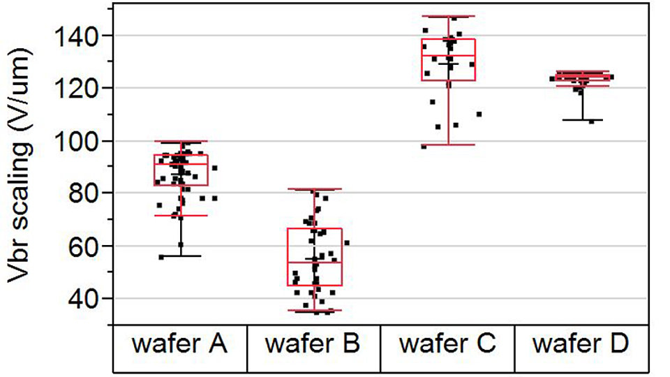
Fig. 2. Breakdown voltage scaling in V per µm gate-drain separation for four different GaN-on-Si wafers.
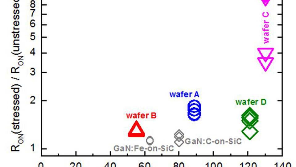
Fig. 3. Dynamic on-state resistance increase in relation to the lateral breakdown strength scaling for wafers A to D. RON was determined 0.2 µs after switching from 65 V off-state drain bias into the on-state. Results for two FBH-grown GaN-on-SiC wafers (in gray) are given for reference.
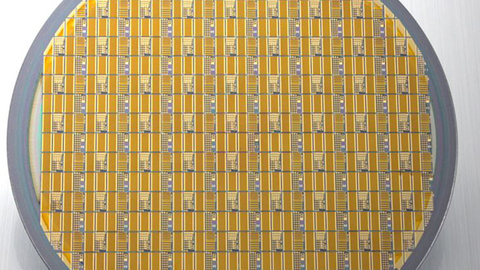
FBH uses a standardized processing scheme for manufacturing GaN-based 600 V / 70 mΩ normally-off switching transistors for power-electronic applications. 4” GaN-on-Si wafers (Fig. 1) from different Japanese and European manufacturers have been used in a recent study. Such wafers open the opportunity for cost-efficient GaN transistors due to reasons of substrate costs and diameters, as well as compatibility with existing Si-device production lines.
However, GaN-on-Si epitaxy for 600 V AlGaN/GaN HFETs is a particular challenge. As compared to other substrate materials (i.e. sapphire or SiC), silicon has a larger lattice mismatch and a larger thermal expansion coefficient mismatch with respect to GaN. This makes the strain management for thick GaN layers crucial and the resulting wafer bowing limits the GaN buffer thickness to approx. 5-6 µm. On the other hand, thick GaN buffer layers are needed for high-voltage isolation since silicon substrates are conductive. Incorporation of deep acceptor traps by using carbon doping is a common approach to still achieve the required breakdown strength. However, the introduced trap states may charge up during high-voltage off-state device condition and the trapped charges degrade the transistor channel conductivity after switching the transistor to on-state. This dispersion phenomenon is known as dynamic on-state resistance (RON) increase. The doping profile and other growth parameter have thus to be adjusted for a feasible compromise between high vertical blocking strength, high lateral blocking strength and low dynamic on-state resistance. This trade-off situation has been analyzed more thoroughly by comparing wafers from 4 different vendors.
High lateral transistor breakdown strengths VBr > 50 V/µm were observed for the different wafers; but VBr deviates by more than a factor 2 (Fig. 2). The breakdown strength is defined as breakdown voltage per gate-drain distance. The used strong buffer doping for obtaining high breakdown strength compromises the dynamic transistor characteristics (Fig. 3). Wafer C has 130 V/µm breakdown strength but the dynamic RON increase (> x3) is not acceptable for efficient switching performance. At the opposite side, wafer B has the lowest dynamic RON increase (~x1.3) but also the lowest breakdown strength (52 V/µm). Wafer D appears as a feasible compromise of moderate dispersion and high VBr.
The trade-off situation between VBr and dynamic RON by is apparent when comparing wafer A and wafer B. The active epitaxial structures are very similar to each other but differ by the on-set of the carbon-doped GaN buffer region that starts at different depths beneath the 2DEG channel; 100 nm for wafer A and 500 nm for wafer B. The thinner non-doped GaN channel of wafer A gives a higher breakdown strength, but trapped charges in the doped buffer are closer to the channel electrons and generate more dispersion.
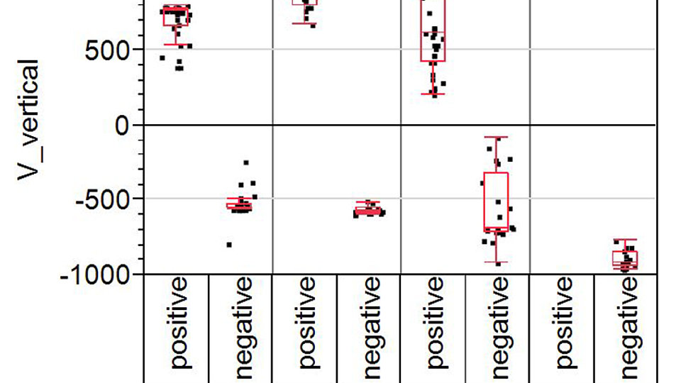
Reproducibility inside the wafers has been found to be an additional problem and this is apparent for the distribution of the vertical blocking strength of the wafers (Fig. 4). +600 V vertical blocking is needed for transistor operation with source-connected substrate. But many probed structures on wafer A and wafer C do not reach this limit although the median vertical breakdown strengths are above +600 V.
In conclusion, only wafer D can be used for manufacturing 600 V GaN switching transistors when considering the performance for vertical blocking strength, lateral breakdown strength and for the dynamic on-state resistance.
Publications
O. Hilt, E. Bahat-Treidel, A. Knauer, F. Brunner, R. Zhytnytska, J. Würfl, "High-voltage normally OFF GaN power transistors on SiC and Si substrates", MRS Bull., vol. 40, no. 05, pp. 418-424 (2015).
O. Hilt, R. Zhytnytska, J. Böcker, E. Bahat-Treidel, F. Brunner, A. Knauer, S. Dieckerhoff, J. Würfl, "70 mΩ / 600 V Normally-off GaN Transistors on SiC and Si Substrates" Proc. 27th International Symposium on Power Semiconductor Devices & IC's (ISPSD 2015), May 10-14, Hong Kong, China, pp. 237-240 (2015).


