Flip-Chip Interconnects for DC to 500 GHz
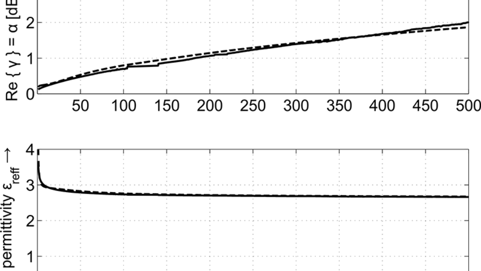
Fig. 3: Propagation coefficient (top) and effective permittivity of the utilized stripline waveguides on the carrier board from on-wafer measurement (solid) and 2D EM simulation (dashed).
Wire-bonding and ribbon-bonding constitute the most common interconnect structures to guide micro- and millimeter-waves (mmW) between MMICs or from MMICs to carrier boards. At W-band (75 to 110 GHz) and beyond, wires/ribbons with sufficiently low insertion loss become impractically small regarding their height and length. To overcome these problems, flip-chip interconnects with low loss up to 500 GHz have been developed. There are two distinct technological challenges related to mmW flip-chip assemblies: 1) the fabrication of the AuSn bumps, and 2) the predictable construction of low loss waveguides on the MMIC and the carrier board. AuSn bumps with diameters of 10 µm and heights of approximately 2 µm are fabricated by the electron beam evaporation method [1, 2]. At mmW frequencies, radiation losses and propagation of undesired higher order modes are the main limiting factors, hence for operation up to 500 GHz shielded striplines have been implemented on MMIC and carrier board [3].
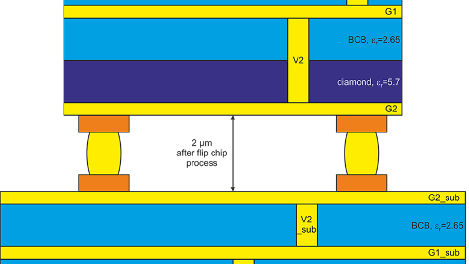
Fig. 1 depicts cross-sectional views of the MMIC/chip and carrier board, which both consist of three Au layers with benzocyclobutene (BCB) as an interlayer dielectric and include Au filled via holes. The MMIC is further equipped with a diamond layer for heat-spreading, when used with InP DHBT power amplifiers. The bulk substrate materials of MMIC and carrier board are aluminum-nitride (AlN) and silicon (Si), respectively.
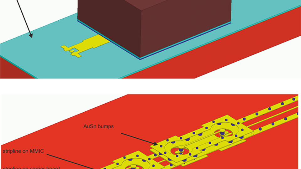
The AuSn bumps connect the chip’s G2 layer with the carrier’s G2_sub layer upon completion of the flip-chip process. Around the signal bump within the flip-chip transition area, several shielding bumps are placed on top of the G2_sub layer, resulting in an electrical “fence” around the signal connection, effectively suppressing radiative leakage losses (Fig. 2).
We have used i-line stepper lithography with 15 μm negative photoresist to create a lift-off resist profile for the subsequent evaporation of 6 μm high (before bonding) and 10 μm diameter eutectic Au80Sn20 bumps. The desired eutectic composition is obtained by alternating between Sn and Au layers in a multilayer scheme with appropriate layer thicknesses. The evaporation sequence ends with a thin gold cap layer to suppress surface oxidation. The AuSn bumps and the underlying electroplated Au interconnect layer G2_sub are separated by a thin TiPtAu diffusion barrier layer, which is patterned in an additional lithographic lift-off step, in order to prevent the unwanted diffusion from Au to Sn. Upon completion of the frontend processes, both 3 inch chip and carrier wafers are mounted on blue tape and diced with a conventional diamond saw. The flip chip assembly is carried out using an FC-150 semi-automatic bonder. The flip-chip bonding temperatures used in this experiment are around 320 to 350°C, and the heating time during bonding is at least 100 seconds in order to transfer adequate heat through the entire BCB stacks to the AuSn bumps.
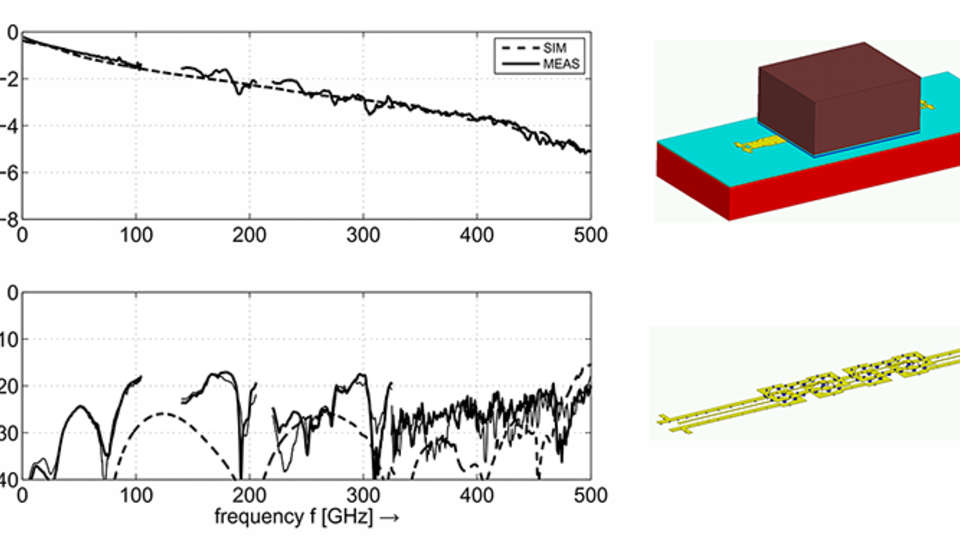
On-wafer measurements of the flip-chip interconnects after multiline Thru-Reflect-Line (mTRL) calibration have been performed. The fabricated stripline waveguides are ideally suited for operating frequencies up to 500 GHz and allow for precise on-wafer calibration, establishing stripline reference planes. Fig. 3 compares the measured and simulated (2D EM) propagation coefficient and effective permittivity of the stripline on the carrier board, which are in excellent agreement. Fig. 4 includes measured and simulated (3D EM) scattering parameters of four stripline-to-stripline flip-chip transitions with a total length of 1.8 mm. Each of the two striplines on the MMIC has a length of 160 µm. At 500 GHz this structure exhibits an insertion loss value of around 5 dB, which means around 1 dB per transition (excluding stripline loss). Return loss values are greater than 18 dB from DC to 500 GHz.
Publications:
[1] S. Monayakul, S. Sinha, C.-T. Wang, N. Weimann, F.-J. Schmückle, M. Hrobak, V. Krozer, W. John, L. Weixelbaum, P. Wolker, O. Krüger, W. Heinrich, „Flip-Chip Interconnects for 250 GHz Modules“, IEEE Microwave and Wireless Components Letters, Vol. 25, No. 6, June 2015.
[2] S. Monayakul, S. Sinha, F. J. Schmückle, M. Hrobak, D. Stoppel, O. Krüger, B. Janke, N. G. Weimann, „Process Robustness and Reproducibility of sub-mm Wave Flip-Chip Interconnect Assembly”, Conf. on Electrical Performance of Electronic Packaging and Systems (EPEPS), San Jose, USA, Oct. 25-28, 2015.
[3] S. Sinha, S. Monayakul, M. Hrobak, R. Dörner, F.-J. Schmückle, N. Weimann, V. Krozer, W. Heinrich, “Theory, Design and Characterization of Broadband Terahertz Interconnects”, IEEE Transactions on Microwave Theory and Techniques, submitted.


