Double helical optical antennas for direct coupling to on-chip waveguides or quantum emitters
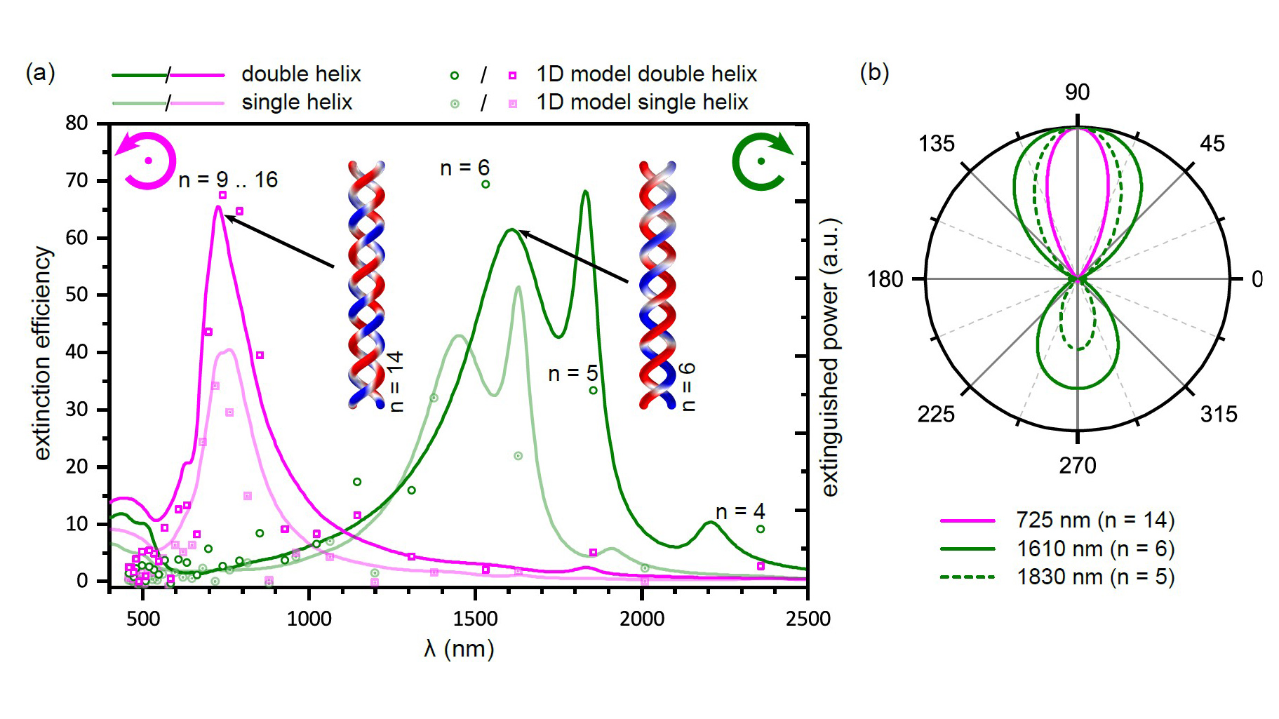
Fig. 1: Modeling far-field response and directional radiation. a) Comparison of extinction efficiencies of free-standing single and double right-handed helices, when excited with right-handed circularly polarized (RCP green) and left-handed circularly polarized (LCP magenta) light. Subplots with normalized surface charge distribution of a high (n = 14) and a low order (n = 6) modes in the double helix show an antisymmetric pattern. Points represent position and power, coupled to the plasmonic modes according to the analytical design tool.
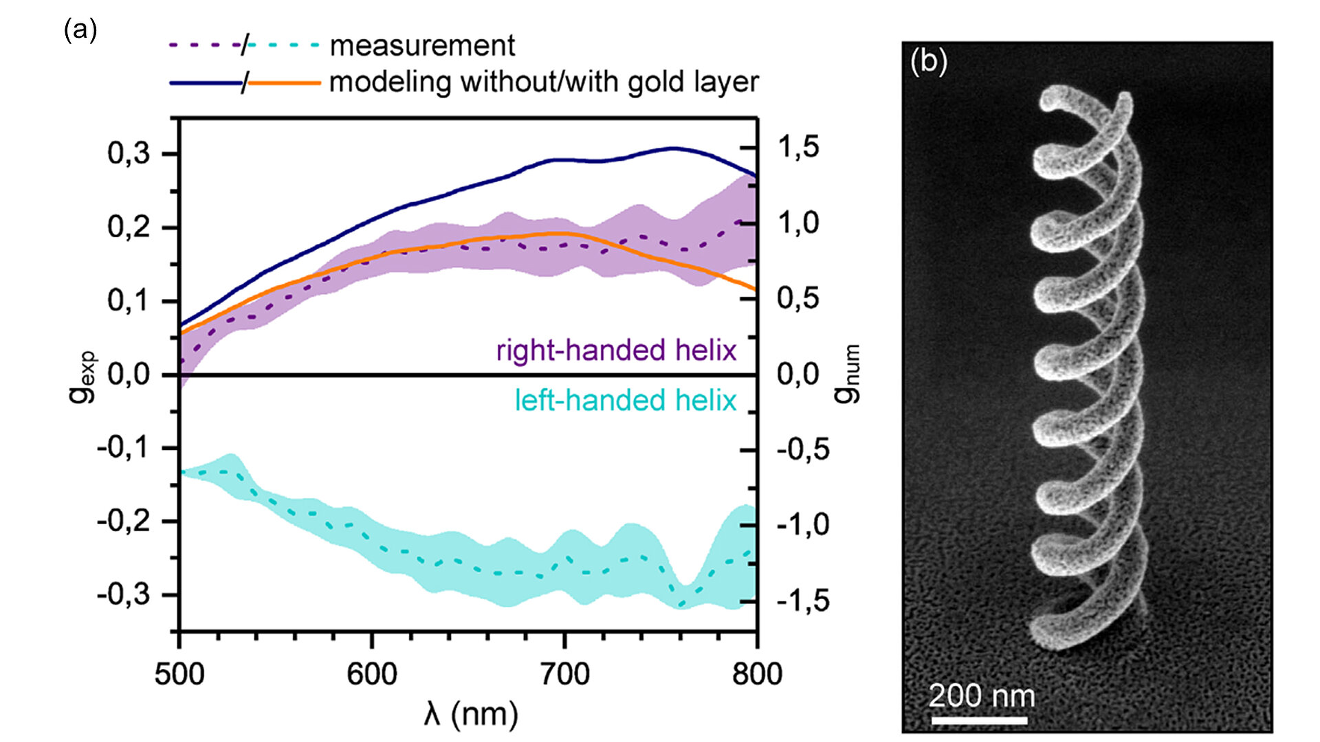
Fig. 2: Fabrication and characterization. a) Comparison of the experimental dissymmetry factor gexp indicating the strength of the chiroptical response of right-handed (violet) and left-handed (cyan) helices with the theoretical gnum obtained by full-field modeling of the transmission setup with the right-handed double helix on the substrate. b) Scanning electron micrograph of the double helix after oxygen plasma cleaning, 45° side view.
Polarization is an important basic property of light related to the spin degree of freedom of its fundamental quanta, the photons. Right and left circularly polarized light corresponds to photons with spin +1 and -1, respectively. Accordingly, controlling the degree of (circular) polarization enables different photonic quantum information protocols. While numerous advanced but macroscopic devices exist for photon polarization control, efficient implementation in future on-chip devices requires a nanoscale solution that combines strong light-matter interaction with a handle for setting or determining the polarization state.
In this regard, metallic nanostructures are advantageous since their free-electron gas can be excited into collective movement by incident light. The associated quasi-particle is named plasmon-polariton and features electromagnetic nearfields at the metal surface. Accordingly, the resonant excitation of a well-designed plasmonic antenna can confine optical fields several orders below the diffraction limit, leading to extreme nearfield concentration. Therefore, plasmonic antennas are attractive both for miniaturized optical devices and for direct coupling to quantum emitters. Helical plasmonic geometries are particularly promising, as they combine a distinct chiroptical response with local field enhancements.
Here, we went a step further by designing and fabricating double helical antennas that can be employed in the visible to near-infrared regime. By using two nanowires instead of one, coupling results in a hybridization of the plasmonic modes to both symmetric (dipole-forbidden) and antisymmetric (dipole-allowed) modes. The antisymmetric mode concentrates the fields between the wires, which allows a direct coupling to 2-wire waveguides as well as to dipolar quantum emitters placed underneath within the substrate. Based on our established understanding of the excitation mechanisms in a single helix, we extended our analytical design tool for double helices. Full-field electromagnetic modeling complements the design and provides insight into the antisymmetric mode patterns (see Fig. 1). The antennas feature a broadband response sensitive to the circular polarization state of light for both the telecom and the visible-to-near-infrared range according to their design [1]. In addition, they radiate strongly directional and act as efficient converters from linearly polarized to circularly polarized light. When coupled to a linearly polarized dipolar quantum emitter, such as a color center in a wide bandgap material, they may act as an ultrabright spin-selective single photon source [2]. Furthermore, coupling to an on-chip waveguide forms an ultrasmall polarization converter.
Fabrication relies on direct electron beam writing [3] using Au(acac)Me2 as gaseous precursor compound (see Fig. 2). This 3D nanoprinting approach allows to place the nanoscale antennas directly at the desired chip-position and provides highly precise geometrical control at the nanoscale. However, since a substantial amount of the carbonaceous ligand material is incorporated during printing, an oxygen plasma treatment is required to obtain a pure gold shell. Finally, the fabricated antennas were optically characterized with respect to their circular dichroism, i.e. the strength of their chiroptical response.
This work was funded by the German Research Foundation (DFG) project “chiralFEBID” under Project ID HO5461/3-1 and by the Swiss National Science Foundation by the COST – SNF project IZCOZ0_205450.
Publications
[1] A. Tsarapkin, L. Zurak, K. Maćkos, L. Löffler, V. Deinhart, I. Utke, Th. Feichtner, K. Höflich, “Double Helical Plasmonic Antennas,” Adv. Funct. Mater., p. 2507471, 2025, DOI: 10.1002/adfm.202507471
[2] L. Kuen, S. Burger, L. Zschiedrich, T. Feichtner, S. Burger, K. Höflich, “Chiral and directional optical emission from a dipole source coupled to a helical plasmonic antenna,” Appl. Phys. Lett., vol. 124, p. 231102, 2024, DOI: 10.1063/5.0201748
[3] I. Utke, P. Swiderek, K. Höflich et al., “Coordination and organometallic precursors of group 10 and 11: Focused electron beam induced deposition of metals and insight gained from chemical vapour deposition, atomic layer deposition, and fundamental surface and gas phase studies,” Coord. Chem. Rev., vol. 458, p. 213851, 2022.