Demonstration of GaN-based near UV laser diodes
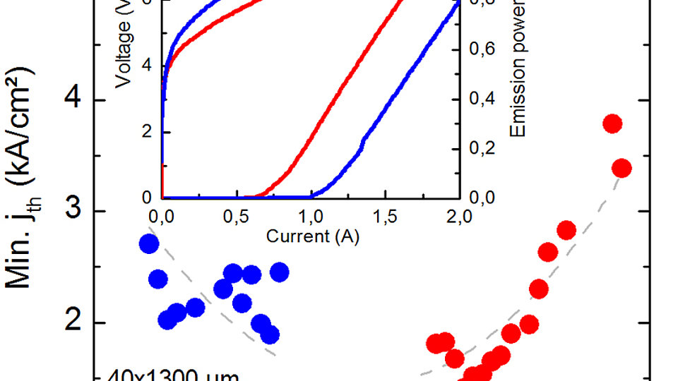
Fig. 1: Minimum threshold current density as a function of emission wavelength of 40x1300 µm BA LDs operated in pulsed mode. Inset: typical LIV characteristics for both heterostructure designs.
The FBH has developed low-threshold gallium nitride (GaN) based edge-emitting laser diodes (LDs) emitting in the near ultraviolet spectral range. The work focuses on the realization of continuous wave (cw) operating LDs with emission wavelengths near 386 nm for applications like spectroscopy, metrology, and lithography. Based on previous developments of blue-violet InGaN quantum well LDs operating in cw mode, we were able to realize laser structures emitting below 390 nm with threshold current densities as low as 2 kA/cm² in pulsed operation.
Fig. 1 shows the minimum threshold current densities of broad area (BA) lasers operated in pulsed mode as a function of the emission wavelength. This includes the previously developed lasers near 420 nm and the newly developed laser diodes in the UV-A wavelength range. In order to obtain these results the heterostructure design was optimized as follows: In the first step, the indium gallium nitride active region was adjusted in order to move the emission wavelength toward the near UV. Although the threshold is slightly higher for short-wavelength LDs, the threshold current densities in the range 2 to 3 kA/cm2 should allow cw-mode laser operation in case the material is processed as ridge waveguide (RW) LD. In the next step, the waveguide design will be adjusted for the shorter emission wavelength to increase the confinement of the optical mode and to reduce the threshold current densities even further.
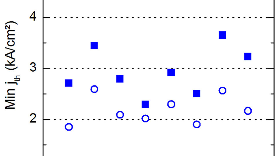
Since the development of RW structures with single mode cw-operation relies on stable and reproducible processes, the stability of the epitaxy as well the chip processing was evaluated. A series of identical epitaxial structures was prepared and processed several times as BA LDs. Fig. 2 shows the variation of the minimum and the median threshold current density in pulsed operation for the different samples and process runs. In addition, identical heterostructure wafers were processed differently in order to improve the laser fabrication process. E.g. the cleaving of the GaN substrates into laser bars was changed in sample D from diamond scribing (D:TF3) to a newly developed laser scribing process (D:TF1-2), which promises a higher quality of the cleaved facet and better reproducibility. The data shows that LDs with emission below 390 nm are reproducibly obtained with low threshold current densities for all process runs.
FBH research: 19.01.2015

