Cost-Effective Packaging for 77 GHz Automotive Radar
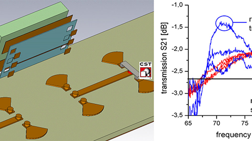
Fig. 1: Example of a 77 GHz interconnect in LTCC flip-chip technology with radial stubs: geometry (left) and thru-line measurement results for the radial and a rectangular stub geometry (right)
Radar systems in the 77 GHz range have become an essential part of the comfort and safety features in high-end cars. They serve as forward-looking sensor for the automatic cruise control, but applications for near-range detection such as parking aid and lane-change assistance are targeted as well.
One of the dominant cost factors for such systems is packaging of the 77 GHz frontend. This becomes even more important if advanced radar concepts such as digital beam forming are applied. Then, the signals from several antennas are processed in parallel, which greatly improves imaging information but requires a higher number of components. Due to this fact, complexity of the frontend increases, both in terms of the amount of chips and the routing of high-frequency and DC connections, and thus demands for adapted packaging as well.
As carrier substrate in the package, LTCC (Low-Temperature Cofired Ceramics) offers interesting possibilities, since it combines multi-level routing capabilities with an acceptable price tag. An LTCC substrate consists of several ceramic layers with metalization levels in between. The chips are placed on top of this layer stack. For this purpose, the flip-chip technique is an advantageous approach. The chip is mounted upside down and the electrical connection to the respective metallic pads on the carrier substrate is realized using metallic bumps. This offers good high-frequency interconnects as well as volume fabrication. However, at 77 GHz, the structures are no longer electrically small and this requires dedicated research efforts in order to achieve the required performance.
As a result of a cooperation with Delphi Electronics and Safety, Kokomo, USA, FBH has addressed this problem and successfully developed suitable interconnect structures between chip and LTCC substrate. What makes the task challenging is the combination of different constraints. First, the dimensions of the pads and the metallic structures on the LTCC substrate cannot be shrinked below typically 100 µm without a significant cost increase due to lithography. This leads to the unfortunate situation that the lateral dimensions of the pad-interconnect geometry are in the order of half a wavelength at 77 GHz, which causes severe parasitic effects. Second, in order to save cost, interconnects were to be realized without vias that are commonly used to connect to the lower metalization levels in the LTCC, particularly for electrical grounding. Thus, the vias had to be replaced by structures like the so-called radial stub, which, however, requires larger area than a via and thus creates conflicts with the third constraint, the demand for a compact design.
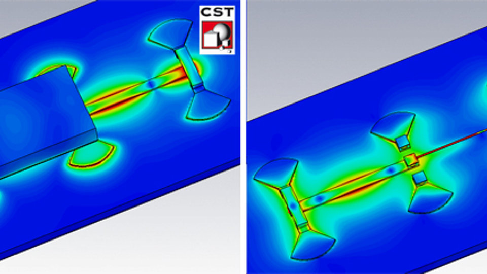
Fig. 1 shows a solution for this problem using radial stubs. A newly developed design with rectangular pads offers sufficient bandwidth and additionally provides improved isolation. The latter quantity describes crosstalk between the different chip interconnects, e.g. input and output of an amplifier, and different elements on the LTCC substrate and is essential for the performance of the radar frontend. Fig. 2 presents a field plot related to this issue. One observes a typical parasitic effect, a surface wave propagating along the top side of the chip thus contributing crosstalk. Such effects are characteristic for chip packaging in the mm-wave frequency range and need to be suppressed by proper design.
Publication:
F.J. Schmückle, U. Pursche, W. Heinrich, Joe Purden, "A 77 GHz Broadband Flip-Chip Transition on LTCC Submount", IEEE MTT-S Int. Microwave Symp.Dig., vol. 1, 2010, pp. 453-456.
FBH research: 25.01.2011

