Brightness and efficiency scaling of a 1 kW, 780 nm diode laser module for additive manufacturing of aluminum
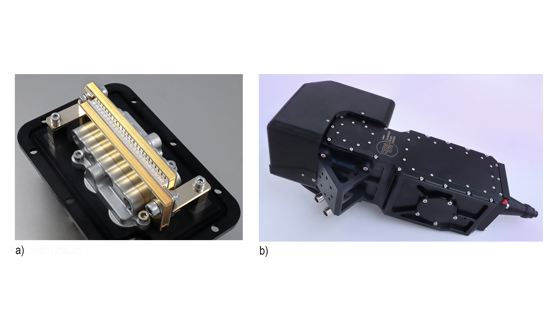
Fig. 1: a) Fully assembled stack module on a base plate. b) Fully assembled process head.
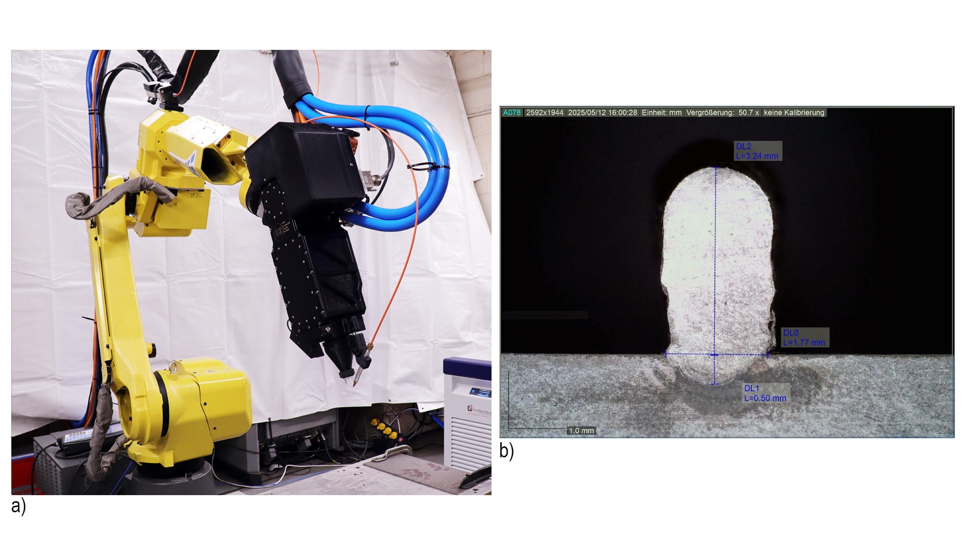
Fig. 2: a) First-generation direct-diode SAMBA AM process head mounted on a robotic arm at the PLM industrial facility. b) Cross-section of an example ten-layer 3D-printed test structure.

Fig. 3: a) Performance characteristics for SAMBA direct-diode AM process heads, using generation I (factory unit) and generation II (lab demonstration) chips: voltage, current and efficiency characteristics of a process head. b) Linearly scaled false color intensity plot of the imaged beam in the focal plan (process spot).
Additive manufacturing (AM) is of increasing interest across industries and research because it enables the layer-by-layer fabrication of complex macroscopic objects that are challenging or impossible to manufacture through traditional machining. Many techniques have been developed over the last years. One successful technique is laser-based AM, which uses high-power laser radiation to melt a metallic wire directly onto a substrate, placing material only where desired. Established laser systems make use of fiber or YAG-lasers but have a large footprint. They also require a fiber to deliver the laser power to the work surface, which is failure-prone – especially when used to process very large structures, such as train side walls. Moreover, the emitted wavelength of 10xx nm is only weakly absorbed in most metals.
FBH scientists, together with their industrial partners, have made strong progress in an alternative approach: direct-diode AM laser modules tailored to address the shortcomings of existing systems. These advances were reported at the CLEO/Europe conference and Laser World of Photonics trade show in Munich. The FBH team presented a compact, continuous-wave 1 kW direct-diode process head, operating at 780 nm, the wavelength at which aluminum has an absorption maximum. The system incorporates highly efficient GaAs-based diode lasers with very wide apertures, so that they emit high per-chip powers [1]. The devices are sandwiched between two heat sinks and then stacked together. Large-channel water coolers extract heat from the sides to form a stack module (Fig. 1a) [2]. Each diode laser is individually fast-axis collimated, and its design tailored so that the beam emitted from the stack is symmetric and matched to the application. For first-stage power scaling, two of these stack modules are geometrically combined. Further power scaling via polarization beam combining remains possible. The process head (Fig. 1b) also includes beam-shaping optics to deliver the beam to the work surface and an in-path camera for visual process control.
A first-generation process head has been transferred to the project partner Photon Laser Manufacturing (PLM). It is mounted on a robotic arm with a control software made by the project partner SKDK GmbH. The assembly delivers 1 kW CW in a 1 mm2 spot. At the conference, we reported first results of AM trials using this new process head: a test structure was 3D-printed on a substrate with a wire-feeding speed of 7 mm/s. The resulting structure is 3 mm in height and was made of 10 layers of melted metal. The factory-mounted system and these initial results are shown in Fig. 2.
Parallel to process demonstrations, the team worked to scale module conversion efficiency and brightness by optimizing the diode lasers themselves. Devices with a narrower stripe width (1.2 mm → 0.8 mm), shorter resonator length (6 mm → 4 mm), and higher front-facet reflectivity (0.8 % → 4 %) were assessed – without changing the epitaxial layer structure. In a laboratory demonstration using two stack modules, we showed that these changes increased the conversion efficiency from 35 % to 50 % at 1 kW (Fig. 3a) and halved the spot size from 1 mm2 to 0.5 mm2 (Fig. 3b). As a result, the power density in the focal area doubled, increasing from 1 kW/mm2 to 2 kW/mm2.
This work was supported through the "AMBER ProFIT Innovation" project SAMBA which is co-financed by the European Fund for Regional Development (ERDF) Berlin under contract number 10193579.
Publications
[1] S. Arslan, P.S. Basler, B. King, J. Glaab, A. Maaßdorf, D. Martin, A. Knigge, A. Ginolas, S. Kreutzmann, P. Crump, “High Power CW 780 nm Diode Lasers for Use in Additive Manufacturing”, Conf. on Lasers and Electro-Optics/Europe and European Quantum Electronics Conf. (CLEO/Europe-EQEC 2023), Munich, Germany.
[2] M. Hübner, S. Arslan, L. Wittenbecher, J. Zender, B. Eppich, D. Martin, P. Della Casa, A. Ginolas, P. S. Basler, N. Lobo-Ploch, P. Crump, M. Rozycki, A. Schultze, U. Tradowsky, A. Knaub, H. Alder, “Compact 1 kW diode laser process head emitting at 780 nm for the efficient direct additive manufacturing of aluminium”, Proc. of SPIE, vol. 13345, High-Power Diode Laser Technology XXIII, Photonics West, San Francisco, USA (2025).
[3] M. Wilkens, S. Arslan, M. Hübner, L. Wittenbecher, J. Zender, B. Eppich, D. Martin, P. Della Casa, A. Ginolas, P. S. Basler, N. Lobo-Ploch, M. Rozycki, A. Schulze, U. Tradowsky, A. Knaub, H. Alder, and P. Crump, “Improved compact 1 kW diode laser module emitting at 780 nm for the efficient direct additive manufacturing of aluminium”, Proc. CLEO/Europe-EQEC, Munich, Germany, Paper CB-8.5 (2025).