Benchmarking of AlGaN/GaN epitaxial wafers for microwave power devices
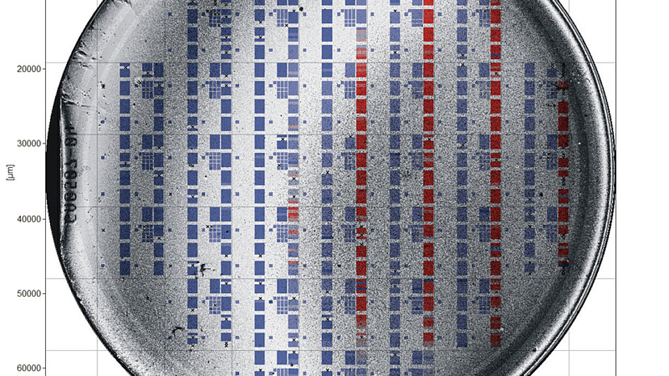
Optical characterization of GaN/AlGaN layers (Candela map) superimposed with a yield map after processing. dark blue = weak devices with low breakdown voltage, light blue/red = high performance devices: substrate and/or epitaxial properties immediately influence device performance.
Design and quality of AlGaN/GaN epitaxial layers in high power microwave devices and MMICs decisively determine their performance and reliability. In order to obtain an unbiased information on the world-wide state of the art of epitaxial layer performance and quality, the European Space Agency (ESA) called for a project to evaluate wafers from different epi-vendors world-wide by means of a stable and reproducible GaN HFET process. The FBH has been selected by ESA to perform this challenging project. Commercially, this task is very sensitive and bound to certain conditions with respect to dissemination of results since the epitaxial vendors involved are competitors on the market. Therefore, only selected and strongly anonymous results can be presented to the public. Recedntly, the project has been successfully finished revealing very interesting results which have been partly published [1].
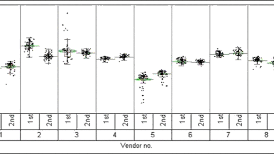
To perform a fair benchmarking from different vendors, FBH at first defined an AlGaN/GaN HEMT epi-structure suitable for L- up to X-band device applications and agreed on this structure with 9 vendors world-wide (5 European, 2 US and 2 Japanese companies or institutions). Thus, identical starting conditions have been obtained for each of the vendors. This epi structure has then been grown on si-SiC by each of the vendors and delivered to FBH for extensive material characterization and, after device processing, for device performance and reliability studies. To minimize the risk of unwanted process variations, the wafers have been split up into two subsequent process runs.
In a first step, extensive non-destructive material characterization has been performed. These included wafer bow measurements, surface roughness measurements, X-ray diffraction to gain information on thickness and composition of the AlGaN/GaN layers and optical defect characterization techniques such as Candela. All measurements were performed on each wafer in order to fully compare the epitaxial layer properties. After device processing a full DC and RF characterization of the devices has been conducted providing data on internal contact and sheet resistances, maximum device current levels, pinch-off and breakdown voltages, leakage current levels as well as microwave properties such as gain, maximum power and device efficiency. All data have been mapped all over the wafer so that a full statistical characterization of the wafer including variations of wafer periphery is available. The work was completed by reliability measurements on selected wafers.
Well performing devices gained from this project have been delivered for ESA's Alphasatmission. Within this project, GaN devices from a European manufacturer will be tested under space conditions for the first time. The devices have already been successfully tested in terms of their electrical and stability performance [2]. They are now incorporated in flight modules and are currently subjected to vibration tests for rocket launch simulations.
Publications:
[1] P. Kurpas, I. Selvanathan, M. Schulz, H. Sahin, P. Ivo, M. Matalla, J. Splettstoesser, A. Barnes, J. Würfl, "Stable and reproducible AlGaN/GaN-HFET processing highly tolerant for epitaxial quality variations", Conf. Dig. CS MANTECH 2010, Portland, USA, May 17-20, pp. 141-144 (2010).
[2] H. Mostardinha, P.M. Cabral, N.B. Carvalho, P. Kurpas, M. Rudolph, J. Würfl, J.C. Pinto, A. Barnes, and F. Garat, "GaN RF Oscillator Used in Space Applications", Workshop on Integrated Nonlinear Microwave and Millimeter-Wave Circuits (INMMIC2010), Goteborg, Sweden, April 26-27, pp.50-53 (2010).
FBH research: 26.10.2010

