Precise measurements with high spatial resolution for optimized violet-blue GaN laser diodes
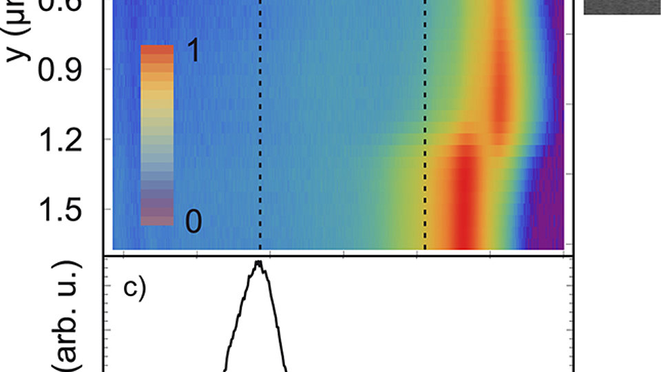
(a) Photoluminescence line scan at laser diode's front facet measured along growth direction y, step width 50 nm, (b) scanning electron micrograph (backscattered secondary electrons) plotted on the same y-scale as (a), bright layer at y = 0 stems from indium-containing quantum wells (c) single spectrum as taken at y= 0, white line in (a)
GaN-based lasers emitting in the blue and violet spectral range still show – compared to lasers in the infrared spectral range – a lower optical output power and a lower efficiency. To improve the laser parameters, the investigation of the optical properties and the defect structure of the active layers of these lasers is of crucial importance. Since these lasers contain layers with thicknesses in the nanometer range, investigations of the optical properties on the laser facets with conventional methods are very difficult.
In cooperation with the Max Born Institute for Nonlinear Optics and Spectroscopy violet-blue laser diodes (wavelength = 420 nm) from the FBH were investigated for the first time with a very high spatial resolution using scanning nearfield optical microscopy (SNOM). Through a glass fiber with a tip of < 50 nm in diameter the layer structure of the violet-blue lasers is optically excited at the front facet. The optical response of the semiconductor layers (photoluminescence) is detected via the same glass fiber. Thus, the optical properties of single layers can be inspected in growth direction as well as in a direction perpendicular to it. From the two-dimensional intensity and wavelength distribution conclusions can be drawn regarding homogeneity, e.g. of the layer composition, as well as the defect structure in the layer sequence. By using electrical contacts to the laser diode additionally to the optical signal the electrical response, the photocurrent, can be detected. This measurement is conducted simultaneously with the photoluminescence at the same place on the front facet.
From both measurements information can be obtained about the built-in potential profile, waveguide modes and the influence of defects on the carrier distribution. The resulting knowledge is then used to further optimize the layer structure of the violet-blue laser diodes.
Publication:
S. Friede, S. Kuehn, J.W. Tomm, V. Hoffmann, U. Zeimer, M. Weyers, M. Kneissl, T. Elsaesser, "Nano-optical analysis of GaN-based diode lasers", Semicond. Sci. Technol., vol. 29, no. 112001 (2014).
FBH research: 07.10.2014
