Plasmonic GaN Detectors for THz Frequencies
Transistor devices for room-temperature signal detection and heterodyne reception at terahertz (THz) frequencies have recently demonstrated excellent performance and are an alternative to diodes. Transistor technologies offer the advantage of monolithic integration into large integrated arrays with direct antenna coupling. This makes them not only more robust, but enables also more compact devices. Furthermore, it has been known since several years that charge transport in the channel of field-effect transistors can show plasma-wave behavior, in particular at terahertz (THz) frequencies. These effects can be used to operate electronic devices beyond their cut-off frequencies. As is well documented in the recent literature THz signals can be detected using conventional CMOS or III-V semiconductor transistors. The THz range offers various applications in biology, medicine, and industry because many materials have a characteristic spectral fingerprint at these frequencies or are transparent. GaN high-electron mobility transistors (GaN HEMTs) have demonstrated particular potential for use as THz detectors, due to their high mobility and breakdown voltage.
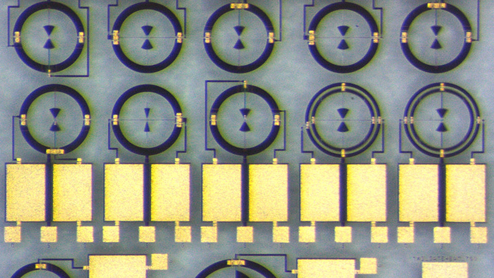
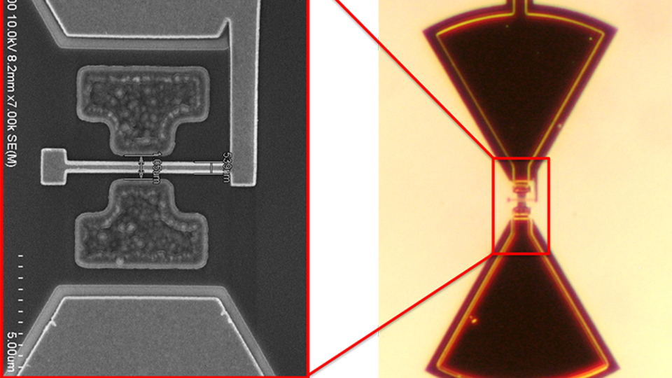
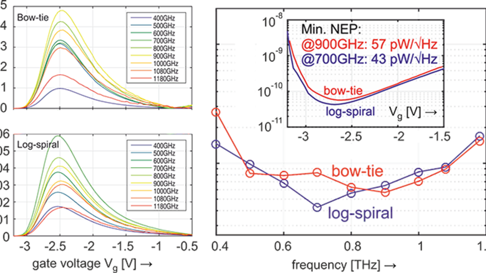
In cooperation with the Goethe-Universität Frankfurt, FBH has initiated several activities in this field, targeting the improvement of detector sensitivity. In 2014, a project on THz detection has started which is funded by the Leibniz Association. This project uses the FBH GaN MMIC process and aims at developing broadband antenna integrated detectors. To achieve this, different types of epitaxial structures, transistor layouts and antenna structures are investigated. This gives the unique opportunity to tailor both transistors and antenna structures for use up to several THz. Fig. 1 illustrates a chip fabricated with several experimental transistors and antennas using bow-tie and log-spiral type antennas. The close-up of a bow-tie structure with a GaN HEMT in its center is presented in Fig. 2. The GaN HEMT has a gate width of 3 µm and a gate length of 250 nm. Broadband measurement results are plotted in Fig. 3 for bow-tie and log spiral structures. They show excellent optical noise equivalent power (NEP) values with peak values of 57 pW/√Hz @ 900 GHz for the bow-tie structure and 43 pW/√Hz @ 700 GHz for the log-spiral structure, respectively.
Publication:
M. Bauer, A. Rämer, S. Boppel, S. Chevtchenko, A. Lisauskas, W. Heinrich, V. Krozer and H.G. Roskos High-Sensitivity Wideband THz Detectors Based on GaN HEMTs with Integrated Bow-Tie Antennas Proc. 10th European Microwave Integrated Circuits Conf. (EuMiC 2015), Paris, France, Sep. 7-8, pp. 1-4 (2015).


