Normally-off GaN transistors with low on-state resistance
GaN-based high-voltage switching transistors enable particularly efficient power converters due to their low area-specific on-state resistance and low gate capacitance. Due to lower losses per switching cycle, GaN-based converters can operate at higher frequencies than converters with Si-based switches. They therefore enable more compact and light-weighted converters. Several 100 V blocking voltage and on-state resistances less than 100 mW are needed for kW-range power converters. The required large device structures consume several mm2 chip area and challenge the quality of the hetero-epitaxy grown semiconductor layers as well as the device processing robustness.
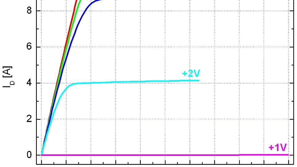
The FBH realized normally-off 300 V GaN transistors with only 80 mW on-state resistance for the opened transistor biased at +5 V gate voltage. The chip size is 4.5 mm × 2.4 mm. The maximum pulse current of >50 A required a transistor gate width of 156 mm. In off-state, the transistor blocks 300 V at 0 V gate bias with a leakage current of less than 50 µA.
The devices have been realized on n-type conductive 3" SiC substrates and thus demonstrate sufficient isolation of the grown GaN semiconductor layer. This is one of the prerequisites to successfully transfer such GaN technology to Si substrates. The larger available diameters (6"-8") and lower costs then open an economical perspective for GaN-based power electronics in competition to traditional Si-based power transistors.
Publication:
O. Hilt, F. Brunner, E. Cho, A. Knauer, E. Bahat-Treidel and J. Würfl, "Normally-off High-Voltage p-GaN Gate GaN HFET with Carbon-Doped Buffer", Proc. Int. Symp. on Power Semiconductor Devices & IC's (ISPSD), San Diego, CA, May 23-26, pp. 239-242 (2011).
FBH research: 23.12.2011

