New equipment for the separation of UV LEDs
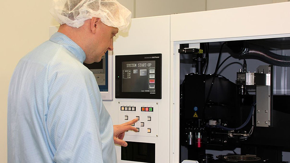
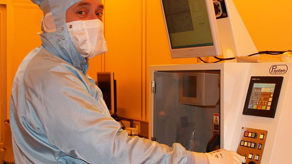
Within the project „Improved efficiency of the process flow for UV LEDs – FBH”, an important part of the Twenty20 program „Advanced UV for Life“, new equipment for the separation of UV LED chips could be purchased and put into operation. With the installation of a laser scriber and a wafer breaker, which were specifically designed for the requirements of sapphire and AlN machining, the technological basis for an efficient chip production has been established.
Sapphire is used as substrate in the UV LED chip production. Due to its hardness new dicing processes for die separation are needed. To use as much as possible of the precious wafer, there are only narrow dicing streets on the wafer. Conventional cut off grinding methods as used for silicon wafer dicing and mechanical diamond scribing with breaking are reaching their limits.
At FBH, a laser-assisted technique was developed and applied to separate UV LEDs. A trench which is aligned to the component structures on the wafer and used as breaking line is created by laser ablation. However, the sapphire substrate is transparent at the wavelength of 355 nm of the nanosecond-pulsed laser applied and high laser pulse energy is required to remove material by multi photon absorption. Processing time is longish and the material ejected from the trench (debris) can contaminate the delicate wafer surface reducing die yield.
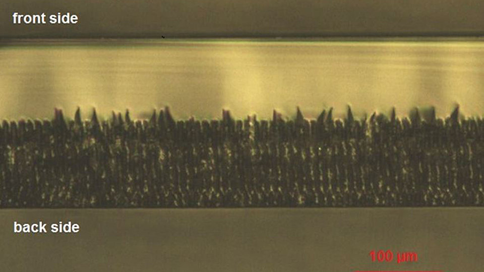
With the new method yield and throughput of sapphire substrate dicing shall be improved. Now, a picosecond laser with 532 nm wavelength and a power of 8 W (40 µJ/pulse, pulse duration <10 ps, 200 kHz repetition frequency, feed rate up to 400 mm/s) is used. The laser beam is focused into the transparent substrate and weakens it locally without expelling particles. By moving the beam focus and the wafer table, a net of lines is created in the substrate, where the separate wafer breaker tool cuts it into parts. During acceptance tests high quality sapphire dicing as well as improvement of yield and throughput could be demonstrated. Upcoming challenges will be the adaption of the processing technology to the specifics of the devices of FBH and the optimization of manufacturing.


