New deposition tool for excellent silicon nitride layers
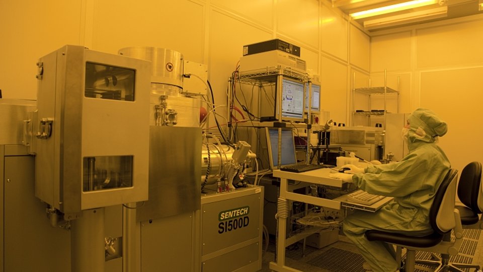
Fig. 1: New PECVD tool for deposition of silicon nitride layers. A load lock allows automatic processing of wafer batches (see left).
With Sentech Instruments' SI500D (Fig. 1) the FBH has a new capable tool for plasma deposition of silicon nitride at hand that significantly expands the institute’s possibilities in this field. In III-V semiconductor technology silicon nitride (SiNx [1]) is preferably used as dielectric, passivation and masking material. Plasma-enhanced chemical vapor deposition (PECVD) is the usual preparation method of silicon nitride layers. The requirements for silicon nitride do not only include basic features such as uniformity, adhesion, sealing as well as thermal and chemical stability but particularly electrical strength. In addition, mechanical strain of the layer (stress) has become a major criterion.
The machine is equipped with an ICP plasma source (Inductively Coupled Plasma) providing high-density non-thermal plasma for the reaction of the precursors silane and ammonia. As a consequence, high temperatures of >300°C can be avoided, which are necessary in parallel plate reactors to produce high-quality SiNx layers. In addition, the energy attracting ions towards the wafer can be adjusted by a high-frequency AC voltage that is independent of plasma generation and thus allows to control layer formation.
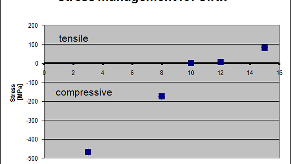
Even though silicon nitride is deposited as an insulating or passivating layer electrical properties of devices may be affected, especially when the functional layers consist of piezoelectric materials such as gallium nitride. Mechanical tension can generate charges and thereby change carrier concentrations in semiconductors. Consequently, the strain of the material is of major importance. On the one hand, the stress of a layer has a thermal origin resulting from different expansion coefficients of the SiNx layer and the underlying substrate. The thermal part of the strain can be reduced by low deposition temperatures. On the other hand, an intrinsic part of stress results from the chemical composition and structure of SiNx. Disorder within the layer structure caused by defects or incorporation of foreign atoms can lead to formation of tensile or compressive stress in the deposited layer. This part of stress can be influenced by appropriately choosing deposition parameters such as pressure, power and silane-ammonia ratio. Fig. 2 shows the effect of pressure on film stress and demonstrates its potential to control, adjust (tensile or compressive) and minimize stress. At a deposition temperature of only 130°C, all layers exhibit a high breakdown field strength of >3 MV/cm. The low deposition temperature also provides the opportunity to coat thermally sensitive photoresist structures with SiNx. This allows, for example, to modify and adjust resist masks for grid etching.
[1] The notation SiNx indicates that the chemical composition of silicon nitride is usually not the stoichometric Si3N4.
FBH research: 03.01.2011

