New class of high-performance THz MMICs – process established at FBH
Recently, FBH has established an InP-based process with operating frequencies up to the 250 GHz range which can be realized on top of a fully processed BiCMOS wafer. This wafer-level hetero-integration technology results in an InP-on-BiCMOS approach, combining the merits of both III-V and Si technologies. This outcome of the research cooperation between the Leibniz institutes FBH in Berlin and IHP in Frankfurt/Oder enables a new class of high-performance MMICs. The hetero-integrated semiconductor technologies employed consist of the IHP SiGe-BiCMOS process in a high-performance 0.25 µm technology with npn-HBTs up to fT/fmax = 180/220 GHz and the FBH transferred-substrate (TS) InP-DHBT technology with fT/fmax values of 359/344 GHz (for a 1-finger HBT with an emitter area of 0.8 × 5 μm2).
First circuits have been realized in this technology with record performance. They comprise a voltage-controlled oscillator (VCO) in BiCMOS technology operating at 48 GHz and 82 GHz, respectively, and InP doublers, triplers, and power amplifiers at frequencies up to 246 GHz.
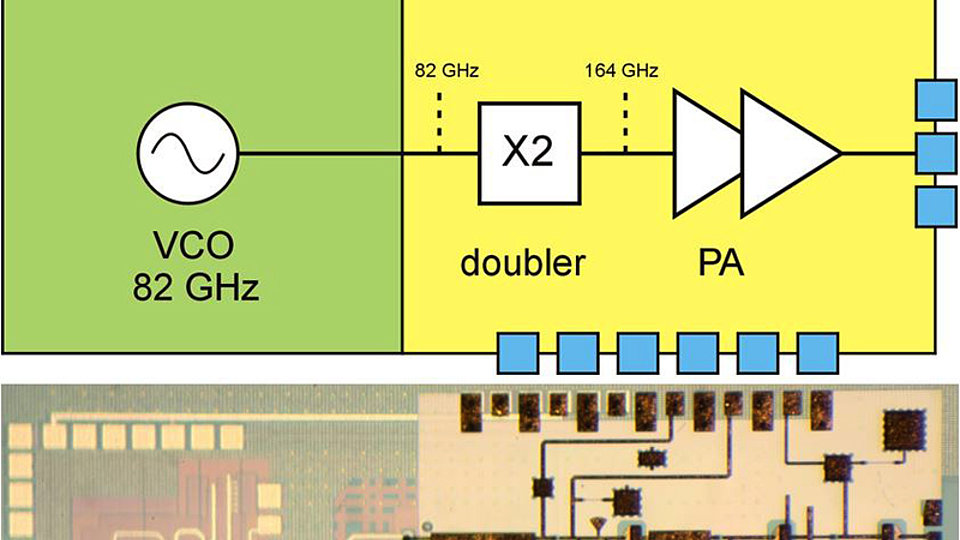
As an example, a VCO in BiCMOS technology operating at 82 GHz integrated with an InP-DHBT frequency doubler and power amplifier is presented. A block diagram of the hetero-integrated circuit and a microphotograph are shown in Fig. 1. The VCO of the combined circuit operates at approximately 82 GHz with an output power of 7.8 dBm, while the InP doubler-amplifier chain delivers 0 dBm at 164 GHz.
A crucial circuit component is the BiCMOS-to-InP transition. Due to the miniaturized structures and thanks to optimization by EM simulations, a return loss better than 12 dB and an insertion loss below 1.0 dB is achieved broadband from a few GHz to 220 GHz.
The TS InP-DHBT part of the circuit consists of a 164 GHz doubler and a 2-stage amplifier. All three stages use the same 2-finger HBT with an emitter size of 0.8 × 5 μm2.
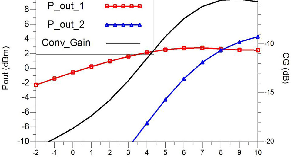
The conversion gain and output power of the first and second harmonic are presented in Fig. 2. The output power of the undesired first harmonic is quite constant at 0-2 dBm for the input power range from 0 to 10 dBm. For an expected VCO power of 6-7 dBm, the second harmonic output power is simulated to be around 0 dBm.
The measured output power is 0 dBm, which is in good agreement with the expected value simulated in Fig. 2. This is the first circuit of this type in this frequency range. The circuit also exhibits record performance when compared to G-band VCOs with a doubler/quadrupler entirely in InP technology.
Publications:
T. Jensen, T. Al-Sawaf, M. Lisker, S.Glisic, M. Elkhouly, T. Kraemer, I. Ostermay, C. Meliani, B. Tillack, V. Krozer, W. Heinrich, "A 164 GHz Hetero-Integrated Source in InP-on-BiCMOS Technology", Proc. European Microwave Conf. 2013, 7-11 Oct. 2913, Nuernberg, German.
T. Kraemer, I. Ostermay, T. Jensen, T. K. Johansen, F.-J. Schmueckle, A. Thies, V. Krozer, W. Heinrich, O. Krueger, G. Traenkle, M. Lisker, A. Trusch, P. Kulse, B. Tillack, "InP-DHBT-on-BiCMOS Technology with fT / fmax of 400 / 350 GHz for Heterogeneous Integrated Millimeter-Wave Sources", IEEE Trans. Electron. Dev., Vol. 60, pp. 2209-2216, 2013.

