Modeling InP HBT noise at highest frequencies – a precondition for low noise amplifiers > 100 GHz
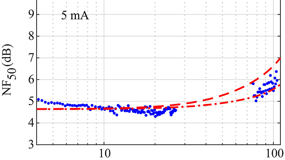
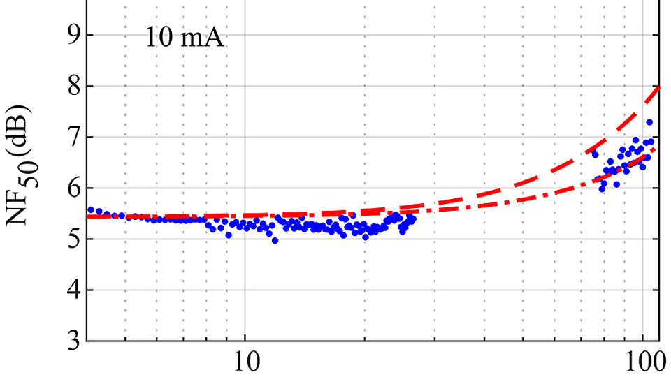
Fig. 2: Measured (bullets) and simulated 50-Ohm noise figure NF50 of a single-finger InP DHBT at Ic = 5 mA, VCE = 1.5 V. Dash-dotted line: a quarter of total time delay, and dashed line neglecting time delay.
InP HBTs are the device of choice for power applications at highest frequencies. The material system easily outperforms silicon-based transistors in terms of speed and power handling capabilities, and the HBT is also superior to HEMT devices since it can operate at higher current densities. The speed of the devices is defined to a large extent by the semiconductor layer stack, which enables to achieve highest cutoff frequencies with rather relaxed lateral dimensions as compared to competing technologies – which translates into lower production cost in small and medium scale series.
Power and broadband amplifiers as well as oscillators were successfully demonstrated on the FBH transfer-substrate InP DHBT process [1] [2]. But even though HBTs are known to have a higher noise figure than HEMT devices, it might be advantageous to use the InP HBT technology to realize low-noise amplifiers, e.g. in order to realize an integrated transceiver front-end chip.
Successful circuit design requires accurate models, and therefore, the noise of the transfer-substrate InP DHBTs was characterized and modeled. The noise model basically consists of a circuit model of the HBT augmented by noise sources describing the thermal noise of the resistances and shot noise at the pn junctions. As the shot-noise power is directly linked to the DC current and the chip temperature controls the thermal noise, noise modeling remains tedious only for the following two reasons: the high frequencies require highly accurate modeling of distributed effects, and the correlation between the shot-noise sources needs to be known very well. The first issue is not specific to noise, and highly precise compact models are available. The second issue is related to the question of how close the noise of the base-collector junction is correlated to the noise originating in the base-emitter junction. It is assumed that the shot noise at both junctions originates basically from the same current and can therefore be considered to be correlated. The correlation is linked to the base-collector transport time and can be described by an equivalent noise correlation time delay τn. This time constant can vary between a fraction of the base-collector transit time τbc down to ωτn ≈ 0, with ω denoting all technically relevant angular frequencies. The latter is a common assumption implemented in traditional large-signal noise models since it is very easy to code.
The only degree of freedom in the noise modeling therefore is the noise correlation time constant τn, which requires to be determined from measurement. For III-V HBTs, we found τn to almost equal the time-delay τbc of a InGaP/GaAs HBT operating at L-band, but to decrease to a small fraction of τbc with shrinking layer thickness and increasing cut-off frequencies for these devices [3]. The investigation of the transfer-substrate InP HBTs supports these results, as τn is found to be small enough compared to τbc to be neglected [4]. The figure proves the extrapolation capabilities of our model well beyond 100 GHz. It shows the noise figure measured at 50 Ohm source impedance, which is about 1 dB higher than the minimum noise figure measured at low frequencies. It can be seen that the noise correlation time constant is very low compared to the total transit time, although the noise figure is slightly overestimated by setting τn to zero (dashed line).
With noise parameters obtained for the InP HBTs providing very good noise performance for the type of device and the accurate noise model, designs of low noise amplifiers beyond 100 GHz become feasible.
Publications
[1] T. Shivan, N. Weimann, M. Hossain, D. Stoppel, S. Boppel, O. Ostinelli, R. Doerner, C.R. Bolognesi, V. Krozer, W. Heinrich, "A Highly Efficient Ultrawideband Traveling-Wave Amplifier in InP DHBT Technology", IEEE Microwave Wireless Compon. Lett., vol. 28, no. 11, pp. 1029-1031 (2018).
[2] M. Hossain, N. Weimann, W. Heinrich and V. Krozer, "Highly Efficient D-Band Fundamental Frequency Source Based on InP-DHBT Technology", in: 48th European Microwave Conference (EuMC 2018), Madrid, Spain, pp. 1005-1008 (2018).
[3] M. Rudolph, F. Korndörfer, P. Heymann, and W. Heinrich, "Compact Large-Signal Shot-Noise Model for HBTs", IEEE Trans. Microwave Theory Tech., vol. 56, no. 1, pp. 7–14, (2008).
[4] E. Kaule, R. Doerner, N. Weimann, M. Rudolph, "Noise modeling of transferred-substrate InP-DHBTs", IEEE Intl. Conf. Microwaves, Antennas, Comm., Electronic Syst. (COMCAS), pp. 1–4 (2017).


