Manufacturable 500 GHz flip-chip assemblies
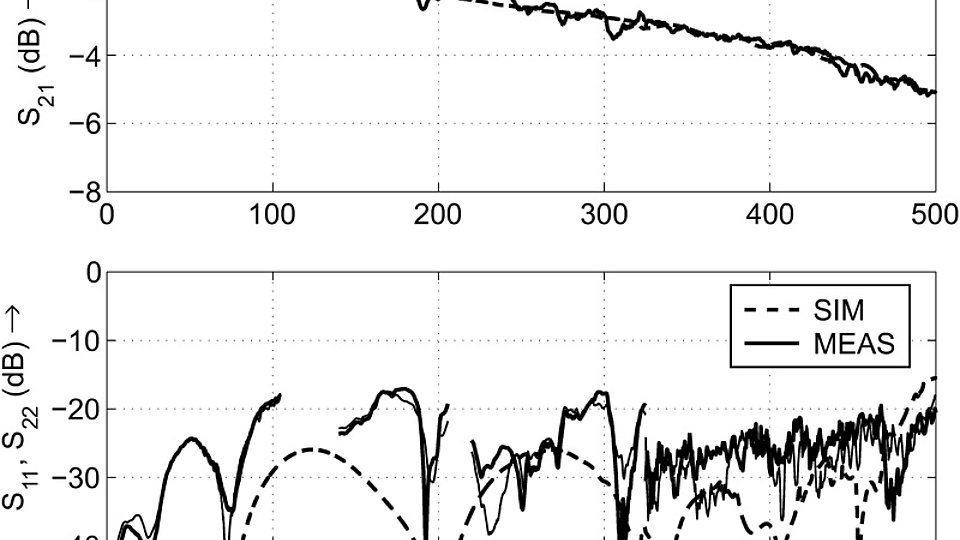
Scattering parameters S21, S11, S22 from on-wafer measurement (solid) and 3D EM simulation (dashed) of four flip-chip transitions connected in series
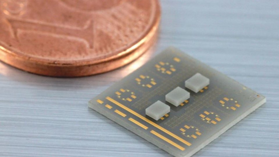
Significant advances have been made to date in the realization of millimeter wave (mm-wave) semiconductor components. Meanwhile, indium phosphide (InP) high electron mobility transistor amplifiers are demonstrating operating frequencies above one terahertz. The use of mm-wave frequencies in commercial applications even between 300 and 500 GHz is hampered, however, by the lack of reasonably priced semiconductor chips and the cost of current mm-wave packaging and subsystem integration techniques. In particular, the bulky split-block packages with waveguide flange connection, which need to be precision-machined to 100 µm accuracy out of massive metal blocks and typically only house one single semiconductor chip, present a roadblock to scalable mm-wave industrial component production.
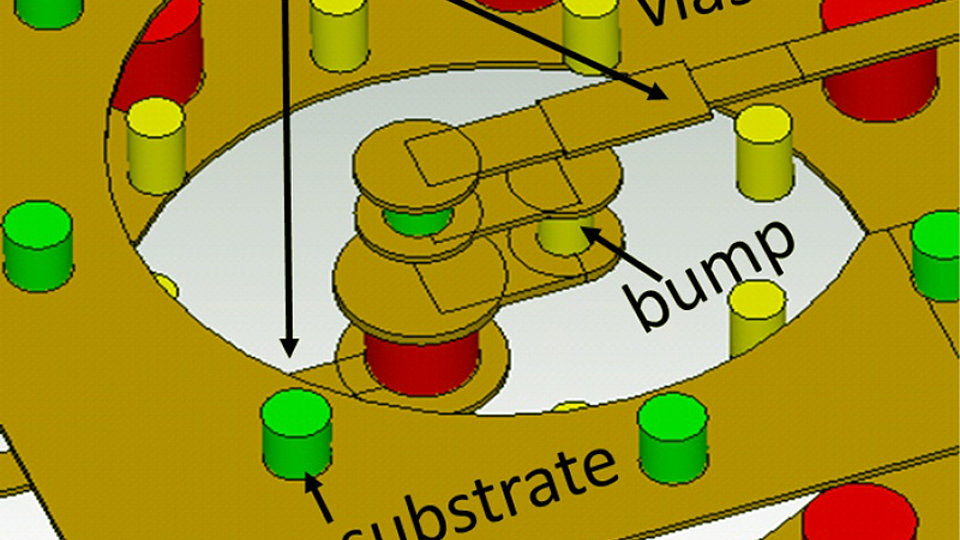
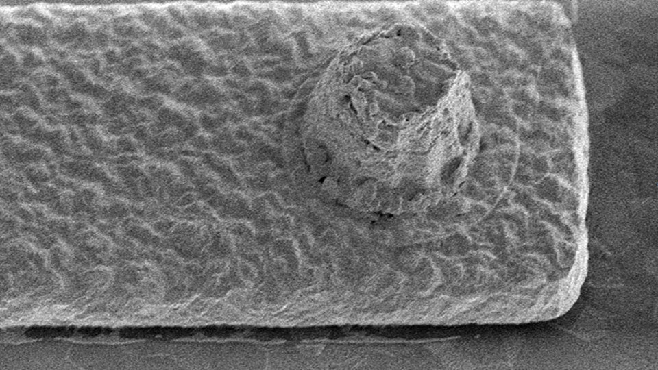
We developed an innovative and manufacturable mm-wave flip-chip mounting architecture by combining the following: First, the diameter of metal bumps that make the mechanical and electrical connection between chip and carrier substrate was scaled down to 10 µm – from typically 50 µm or more. This reduction in size enables a circuit trace width of 10 µm, which is needed for low-loss 500 GHz transmission lines. Secondly, the design of the transmission lines themselves was changed to include an upper and lower electrical shielding in a three-layer gold/BCB interconnection scheme, effectively suppressing radiative losses up to 500 GHz. Finally, the vertical flip-chip transition region was designed to resemble a coaxial line by placing vertical ground connections in a circular pattern around the central signal wire, again confining the fields to avoid radiative losses to the surrounding volume.
The robustness of the assemblies was investigated by calculating the fields within the entire structure comprising of chip and carrier substrate in a 3D-EM simulator, while introducing intentional geometrical offsets – representing fabrication tolerances which would be observed in a practical realization. The experimental validation of the approach showed reproducible low-loss operation across the entire band from DC to 500 GHz, yielding < 1 dB insertion loss per flip-chip transition and > 10 dB return loss across the entire frequency range. Wideband operation of the passive chip mounting structure is desirable to avoid re-engineering of the package for different frequency applications within the mm-wave frequency bands. Moreover, circuit-package interactions can be easier predicted when wideband operation of the packaging structure can be assumed.
The project is funded by the Federal Ministry of Education and Research (BMBF), VIP project AVTE (ref. number 03V0060).
Publications:
N. Weimann, S. Monayakul, S. Sinha, F.-J. Schmückle, M. Hrobak, D. Stoppel, W. John, O. Krüger, R. Doerner, B. Janke, V. Krozer, and W. Heinrich, "Manufacturable low-cost flip-chip mounting technology for 300-500 GHz assemblies", accepted for publication in IEEE Transactions on Components, Packaging and Manufacturing Technology, DOI 10.1109/TCPMT.2016.2636444.
S. Sinha, R. Doerner, F.-J. Schmückle, S. Monayakul, M. Hrobak, N. Weimann, V. Krozer, and W. Heinrich, "Flip-Chip Approach for 500 GHz Broadband Interconnects", accepted for publication in IEEE Transactions on Microwave Theory and Techniques, 2016.


