Line sensors for novel X-ray detectors
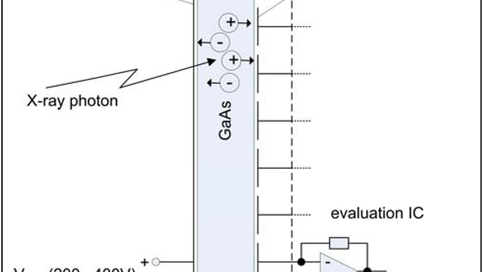
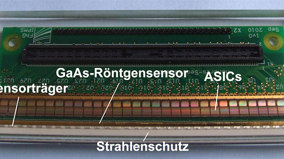
FBH develops line sensors for innovative X-ray detectors in close cooperation with the Electronics Packaging Laboratory (IAVT) at TU Dresden. Only recently, a new generation of direct-converting line detectors has been demonstrated. These devices resolve the disadvantages of present sensor systems comprising scintillator and photo detector. Key benefits are very low crosstalk between adjoining pixels, simple construction and expanded lifetime of the detector chips. Within the system, GaAs sensors directly convert X-ray photons into charge carriers with a lateral resolution of 100 µm per pixel (Fig. 1). The demonstrator comprises a sensor with 1024 pixels and has been set up with assemblies for amplifier and evaluation electronics developed by the Fraunhofer institutes IZFP and IPMS (Fig. 2).
The layout of a 4-level process was developed and realized on 4" GaAs wafers at FBH. The basic devices with 32 pixels received a Schottky contact structure with passivation layer at the front. The backside of the wafer was metalized to obtain an Ohmic contact. These contacts are used to apply the operation voltage of up to 400 V and to read out charge carriers generated by X-ray irradiation. The contact design allows electrical connection both by bonding wires and by flip chip mounting.
The fabrication of about 10 cm long line sensors (1024 pixels) with a regular pixel spacing of 100 microns requires precise positioning of the discrete devices with 32 pixels which makes chip separation particularly challenging (Fig. 3). To obtain a defined gap of 20 microns between two pixels at the joining, chips had to be separated very accurately. Wafers were scribed and cleaved to separate chips that could smoothly be assembled. Sensor chips with 512 pixels were also cleaved by using the same process. With these large chips, only one joining is necessary and the fabrication of an error-free pixel assembly could be simplified.
FBH research: 12.09.2011


