Laser-assisted fabrication of vertical interconnects for AlGaN/GaN power transistors
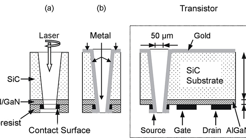
Fig. 1: Scheme of process flow for laser-assisted VIA fabrication. (a) Laser drilling from the backside of the wafer, (b) metal deposition of gold to form an electrical interconnect between front and backside.
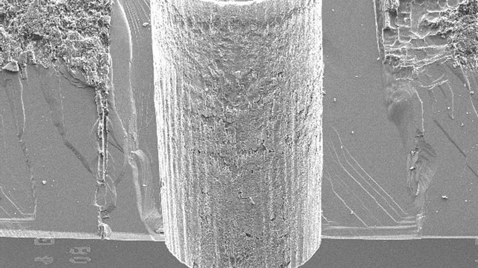
Fig. 2: Scanning electron micrograph of a cross section of a laser drilled hole through 380 µm thick SiC (sample tilted, view of laser exit).
Vertical integration plays a key role with regard to the increasing integration density of electronic devices. Thus, devices can be fabricated with smaller dimensions and reduced electrical losses. Vertical integration leads to a more efficient use of the semiconductor volume and therefore a high specific power density. Low inductivity interconnects minimize switching losses. Vertical interconnect accesses (VIAs) from the device’s front through the substrate down to the backside allow simple and space-saving contacting of the devices in packages.
High-power devices based on the AlGaN/GaN material system are usually fabricated on silicon carbide (SiC). The formation of VIAs, however, is very demanding and time-consuming due to the mechanical hardness and chemical inertness of the SiC substrate material. Dry chemical etching of holes requires mechanical thinning to about 100 µm. Etching of VIAs through thicker SiC is not possible to date. At FBH, a laser-assisted VIA process has been developed that allows the institute the formation of electrical through contacts from the front to the backside of the device on 350 - 400 µm thick SiC. The patented technology was developed already some years ago [PAT] and has recently been optimized for power electronics applications that require larger VIAs with diameters from 150 to 200 µm.
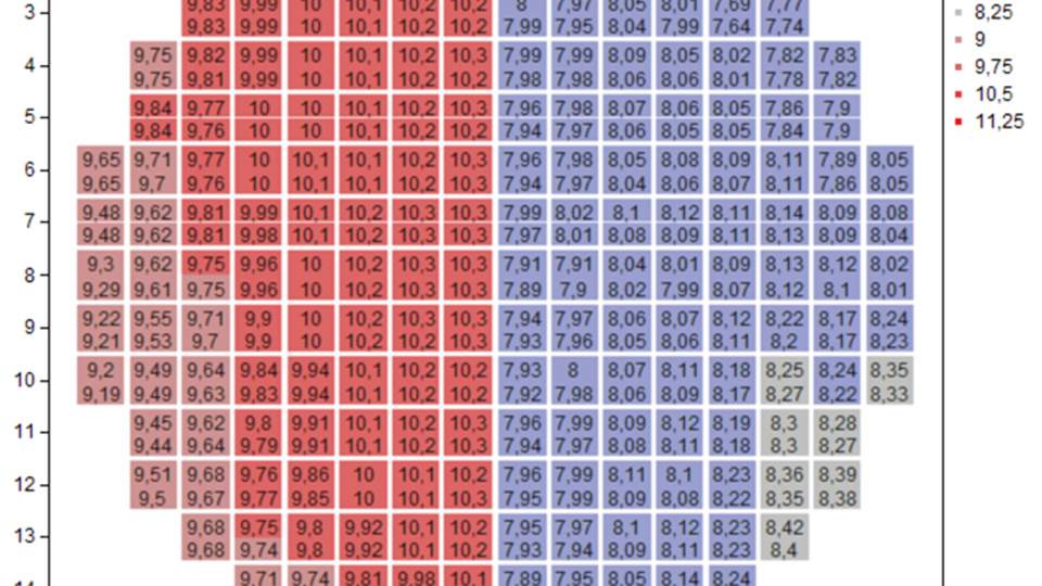
Fig. 1 depicts the process flow. Laser processing is carried out at the wafer’s backside. A solid-state laser with a wavelength of 355 nm providing 4.5 W average output power at 25 kHz pulse repetition rate and a pulse length of < 30 ns is used for laser drilling of through holes. The laser is integrated in a commercial laser workstation (ILS 500 Air) that features a positioning accuracy of the laser beam of ± 1 µm on the wafer’s backside to precisely drill the hole through front contact pads. The laser beam has a diameter of about 15 µm and is appropriately moved across the wafer’s back surface to obtain the desired hole diameters. Thus, it is possible to drill holes with different diameters that can easily be adjusted to needs of the devices or mounting requirements (Fig. 2). Depending on the diameter, the drilling time is about 3 - 5 s per hole. The electrical interconnect is formed by a 5 µm thick gold layer that is deposited onto the wall of the VIA hole. The electrical resistance of a single VIA can be determined from the Ohmic current-voltage behavior. Fig. 3 shows a representative mapping of resistance values of VIAs through 380 µm thick SiC. On the left side of the test sample VIAs with 150 µm diameter were formed, on the right side the VIAs have a diameter of 200 µm. Due to the smaller surface of the wall, the resistance through the 150 µm VIAs is 10 mΩ compared to 8 mΩ obtained from the 200 µm VIAs. The newly optimized process for these larger VIAs will soon be applied to AlGaN/GaN power transistors.
[PAT] Krüger, O.; Würfl, J.; Schöne, G.: Verfahren zur Erzeugung von vertikalen elektrischen Kontaktverbindungen in Halbleiterwafern. Europäische Patentschrift EP 1 891 670 B1, 03.02.2010 (Patentblatt 2010/05).
FBH research: 17.06.2011


