InP-on-BiCMOS integration enables ultra-broadband interconnects
The bandwidth available in microwave and milllimeterwave modules is limited in many cases not by the circuits integrated on the chips but by the packaging approach and the interconnects between the circuits. This is well-known for the conventional wire-bonding technique, but it is true also for advanced approaches such as flip-chip, which, in general, are limited to a frequency range up to 100 GHz. The key criteria determining bandwidth and cut-off frequency of an interconnect are its physical size and the parasitic high-frequency effects associated with it. A simple rule of thumb says: the smaller, the better. Therefore, if one wants to exceed the 100 GHz limit in bandwidth, a new technology is necessary which shrinks the connections between the circuits on the high-bandwidth chips.
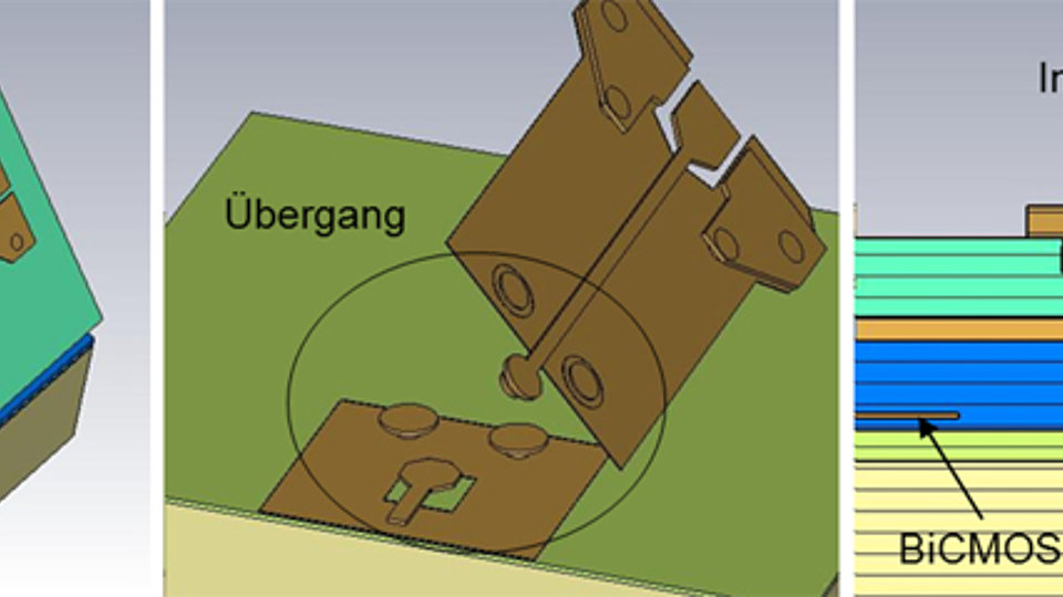
This is the reason why FBH and IHP in Frankfurt/Oder are developing an heterogeneous integration process combining InP-HBT and BiCMOS circuits on the same wafer. Among others, the advantage of this process is that the common integration enables to scale down the dimensions of the interconnects between the circuits. Consequently, their bandwidth capabilities are increased. The vertical distances between the BiCMOS and the InP circuits shrink to 8…10 µm. In order to fully exploit this potential for the interconnect performance it is first of all necessary to define geometry and material configuration in a way such that compatibility with both CMOS and InP technology is fulfilled (see Fig. 1). Secondly, the vias, the metal pattern, and the ground metallization need to be designed by means of 3D em simulation to optimize the high-frequency behavior.
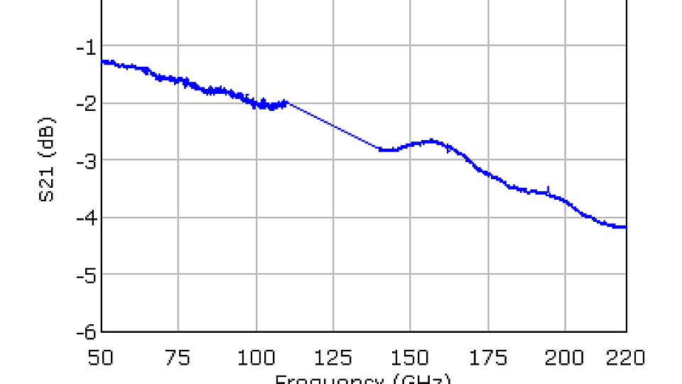
These efforts now proved to be quite successful: We could demonstrate broadband function up to 220 GHz. Fig. 2 presents measurement results for a back-to-back test structure, which includes a 1250 µm long transmission line in the BiCMOS part and two interconnects to the InP layer with on-wafer probing pads. The insertion loss of the entire structure includes loss contributions from the BiCMOS lines, the pads, and the interconnects themselves. In practice, the insertion loss of the transitions turns out to be very small so that it is hardly visible in the overall loss. A conservative estimation yields an upper level for the insertion loss per interconnect of 0.5 dB at 100 GHz and 1 dB at 220 GHz. This is achieved together with excellent broadband properties over the full frequency range.
Reference:
I. Ostermay, F.-J. Schmueckle, R. Doerner, A. Thies, W. Heinrich, O. Krueger, V. Krozer, T. Jensen, T. Kraemer, M. Lisker, A. Trusch, E. Matthus, Y. Borokhovych, B. Tillack, "200 GHz Interconnects for InP-on-BiCMOS Integration", to be presented at IMS 2013, Seattle.
FBH research: 27.03.2013

